Position: Home > Circuit Diagram > Basic Circuit > Index 13
Low Cost Custom Prototype PCB Manufacturer

Basic Circuit

Index 13


Simple Water Detector-Circuit

Published:2013/11/21 20:47:00 Author:lynne | Keyword: Simple Water Detector Circuit

Simple Water Detector-Circuit
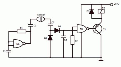
This simple water detector circuit uses alternative voltage in order to prevent the corrosion of the electrodes. It is easy to build and uses N1 as a trigger Schmitt gate which generate the AC. If between the electrodes is a electricity conductor, for example an aqueous solution, then because of the rectification action of D1 and D2, the C4 capacitor is charging. When the capacitor voltage reaches switching threshold of the N2 trigger Schmitt, the relay will trigger and connect, for example a drain pump. The pump will be disconnected as soon as the electrodes won’t touch the liquid. Simple water detector circuit schematic Water detector componentsR1 = 470KR2 = 10M … 22MC1 … C4 = 2.2nFN1, N2 = 1/2 4093D1 … D3 = 1N4148T1 = pnp transistor (BC557)   (View)

View full Circuit Diagram | Comments | Reading(1619)

Telephone Ringtone Generator Circuits

Published:2013/11/21 0:25:00 Author:lynne | Keyword: Telephone Ringtone Generator

Telephone Ringtone Generator Circuits
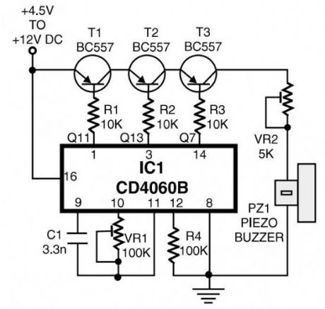
This is a simple home telephone ringtone generator circuit which is built with applying only several electronic components / parts. It generates simulated telephone ringtone and requires only DC supply with 4.5V DC to 12V DC voltage.One may possibly use this circuit in ordinary intercom or phone-type intercom. The sound is pretty loud when this circuit is operated on +12V DC power supply. Even so, the volume of ring sound can be adjusted. Ringtone generator circuit schematic CD4060B is chosen to produce three kinds of pulses. Preset VR1 is fine-tuned to get 0.3125Hz pulses at pin 3 of IC1. At the same time, pulses obtainable from pin 1 will be of 1.25 Hz and 20 Hz at pin 14. The three output pins of IC1 are connected to base terminals of transistors T1, T2, and T3 through resistors R1, R2, and R3, respectively. Working with a built-in oscillator-type piezobuzzer generates about 1kHz tone. In this particular circuit, the piezo-buzzer is turned ‘on’ and ‘off’ at 20 Hz for ring tone sound by transistor T3. 20Hz pulses are obtainable at the collector of transistor T3 for 0.4-second duration. Just after a time interval of 0.4 second, 20Hz pulses become again obtainable for another 0.4-second duration. This is followed by two seconds of nosound interval. Thereafter the pulse pattern repeats by itself.   (View)

View full Circuit Diagram | Comments | Reading(1374)

Gas Leak Detector Circuit

Published:2013/11/21 0:22:00 Author:lynne | Keyword: Gas Leak Detector

Gas Leak Detector Circuit
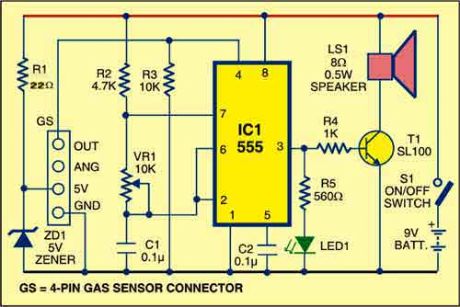
Here is a gas leak detector circuit that detects the leakage of LPG gas and alerts the user through audio-visual indications. The circuit operates off a 9V PP3 battery. Zener diode ZD1 is used to convert 9V into 5V DC to drive the gas sensor module. The gas leakage circuit uses the SEN-1327 gas sensor module from RhydoLABZ. Its output goes high when the gas level reaches or exceeds certain point. A preset in the module is used to set the threshold. Interfacing with the sensor module is done through a 4-pin SIP header. Pin details of the gas sensor module are shown in Fig. 2. An MQ-6 gas sensor is used in the gas sensor module. The sensor can also be used to detect combustible gases, especially methane. Gas leak detector schematic Whenever there is LPG concentration of 1000 ppm (parts per million) in the area, the OUT pin of the sensor module goes high. This signal drives timer IC 555, which is wired as an astable multivibrator. The multivibrator basically works as a tone generator. Output pin 3 of IC 555 is connected to LED1 and speaker-driver transistor SL100 through current-limiting resistors R5 and R4, respectively. LED1 glows and the alarm sounds to alert the user of gas leakage. The pitch of the tone can be changed by varying preset VR1. Use a suitable heat-sink for transistor SL100. google_ad_client= ca-pub-9265205501290597 ;google_ad_slot= 6648404198 ;google_ad_width=336;google_ad_height=280;   (View)

View full Circuit Diagram | Comments | Reading(1277)

Sound Level Meter Circuits

Published:2013/11/19 20:49:00 Author:lynne | Keyword: Sound Level Meter Circuit

Sound Level Meter Circuits
This sound level meter circuit can be used to control the intensity of a sound recording or in a disco. It has 5 measurement domains between 70 and 120 dB; reading accuracy is 0.5 dB. Microphone M1 is used to receive the acoustic signal and is coupled to C1, C2, R1 and R2. This components, together with the microphone’s capacity and with the input impedance of the amplifier form an input filter. The filtered signal goes to operational amplifier IC1 whose sensitivity can be switched with S2 corresponding to the five measuring domains. D1 … D4 diodes rectifies the alternating voltage at the amplifier output and feeds the indicator tool through R9. D5 is used in order to protect the sound level meter indicator against high voltages; it limits the rectifier’s output voltage when the sound level is too high. On normal conditions the input current is about 2 mA that is why the circuit can be powered with 2 x 9V batteries. S1 switch is used to disconnect the sound level meter device after measurement. The indicator tool should have a graded scale in dB with the maximum value of +10. Sound Level Meter Schematic   (View)

View full Circuit Diagram | Comments | Reading(912)

Johnson Ring Counter Circuit with

Published:2013/11/19 20:43:00 Author:lynne | Keyword: Johnson Ring Counter

Johnson Ring Counter Circuit with

Counters have numerous application in Digital field. There are many types of counters, today we are going to explain about Johnson counter. Johnson counter is also called as Inverse feedback counter or twisted Ring counter. It has 2N states where ‘N’ is the number of flip-flops. So here is how to make a Johnson counter using IC 74LS164. Here are some of the features of IC 74164: Gated (enable/disable) serial inputs Fully buffered clock and serial inputs Asynchronous clear Typical clock frequency 36 MHz Typical power dissipation 80 mW Circuit diagram for Johnson counter using IC 74164 is given below: The components needed for this circuit is: 74164 IC 7404 IC ( Inverter ) 35Mhz clock source 5v supply Indicators to indicate the state In above diagram X1 to X8 are indicators to indicate the current state. The 74LS164 IC have 8 flip-flops built-in. So the number of states will be 2 x 8 = 16 states. Below diagram shows the truth table which have 16 states. As you can see that there is only one bit change from one state to another state. Every bit starting from X1 goes high after one state till X8. After X8 is high the X1 bit will go low ( 0 ). This is because in the circuit the output of X8 is given as the input to the NOT gate 7404 IC. And the output which is inverted is given back as an input to IC 74164. Hence Johnson counter is also called as Inverse feedback counter. If you have any doubt in the circuit please leave a comment we will respond you.   (View)

View full Circuit Diagram | Comments | Reading(2275)

First-order Butterworth Active Low-pass Filter Circuit

Published:2013/11/18 20:22:00 Author:lynne | Keyword: Active Low-pass Filter

First-order Butterworth Active Low-pass Filter Circuit
Butterworth filter is a type of filter whose frequency response is flat over the passband region. Low-pass filter (LPF) provides a constant output from DC up to a cutoff frequency f(H) and rejects all signals above that frequency. Circuit diagram shown below is a first-order low-pass Butterworth filter that uses RC network for filtering. Loading of the RC network is avoided by using the Op-Amp which is configured for non-inverting mode. Resistors R1 and Rf determine the gain of the filter. The components needed for this circuit are: Op-Amp ( 5 terminal ) 3 Resistors 1 Capacitor Voltage sources The voltage gain below the high cutoff frequency is called the passband gain. It is given by the formula : Af = 1+Rf/R1 High cutoff frequency is given by the formula : f (H) = 1/(2πRC) In the above circuit the component XSC1 is the Oscilloscope which is used to verify the circuit so don’t get confused with it. In the above circuit the cutoff frequency is decided the resistor R and capacitor C. You can choose any desired value to fix the cutoff frequency. In the above circuit i choose the cutoff frequency to be approximately 5KHz so i used the resistor R of value 10KΩ and capacitor of value 3nF. You can change it if you want to by using the above cutoff frequency formula. The first order low-pass filter has a practical slope of -20 dB/decade. The low-pass filter has a constant gain Af from 0 to high cutoff frequency f (H). At f(H) the gain is 0.707Af and after f (H) it decreases at a constant rate of 20 dB/decade. The frequency f = f (H) is called the high cutoff frequency because the gain of the filter at this frequency is down by 3 dB ( =20log(10) 0.707 ) from 0 Hz. The AC analysis of the above circuit is given below. But it is not exactly for the above circuit. The cutoff frequency is now made 20kHz. For getting cutoff frequency 20kHz you need resistor of value 1KΩ and capacitor of value 7.96nF.   (View)

View full Circuit Diagram | Comments | Reading(1495)

Precision Full Wave Rectifier Circuits

Published:2013/11/18 0:27:00 Author:lynne | Keyword: Precision Full Wave Rectifier Circuit

Precision Full Wave Rectifier Circuits
The use of Operational amplifiers can improve theperformanceof a widevarietyof signal processing circuits. In rectifier circuits, the voltage drop that occurs with an ordinary semiconductor rectifier can be eliminated to give precision rectification. The below shown circuit is the precision full wave rectifier. It consists of following sections: Precision half-wave rectifier Inverting summing amplifier The input voltage Vin is applied to one terminal of the summing amplifier along with resistor R3 and to the input of the precision rectifier. The output of precision rectifier is applied to another terminal of summing amplifier. The precision half-wave rectifier circuit uses an inverting amplifier configuration. When the input signal Vin is positive, Op-Amp output terminal is negative, Diode D1 is reverse biased and D2 Diode is forward biased, the circuit is Vb = -(R2/R1) * Vin In the circuit, R1 and R2 have been chosen such that R2 = 2R1.So the voltage at Vb = -2Vin. Thus during the positive half cycle of the rectified voltage Vb is applied to terminal B of the inverting summing amplifier is -2Vin. The voltage at terminal A is Va = +Vin. The output from the summing circuit with R3=R4=R5 is Vo = – (Va+Vb). Hence Vo = -(Vin – 2Vin) = +Vin. So during the negative half cycle of the input, the Op-Amp output terminal goes positive, causing D2 to be reverse biased. Without D1 in the circuit, the Op-Amp output would be saturated in the positive direction. However, the positive voltage at the Op-Amp output forward biases the D1. This tends to pull the Op-Amp inverting terminal in a positive direction. But, such a move would cause the Op-Amp output to go negative. So, the output settles at the voltage close to ground level. So to be clear, the negative half-cycle is clipped off. That is Vb=0 and Va = -Vin. Totally the Vo will be Vo = -(-Vin+0) = +Vin. It is seen that the output is a full wave rectified version of the input voltage. A Precision full-wave rectifier is also known as absolute value circuit. This means the circuit output is the absolute value of the input voltage regardless of polarity. If you any doubt about the circuit please drop it in comments we will respond you.;   (View)

View full Circuit Diagram | Comments | Reading(1198)

TL496 Circuit

Published:2013/11/18 0:02:00 Author:lynne | Keyword: TL496 Circuit

TL496 Circuit
The TL496C power-supply control circuit is designed to provide a 9-V regulated supply from a variety of input sources. Operable from a 1- or 2-cell battery input, the TL496C performs as a switching regulator with the addition of a single inductor and filter capacitor. When ac coupled with a step-down transformer, the TL496C operates as a series regulator to maintain the regulated output voltage and, with the addition of a single catch diode, time shares to recharge the input batteries.The design of the TL496C allows minimal supply current drain during standby operation (125 µA typical). With most battery sources, this allows a constant bias to be maintained on the power supply. This makes power instantly available to the system, thus eliminating power-up sequencing problems.   (View)

View full Circuit Diagram | Comments | Reading(1202)

USB Power Booster Circuits

Published:2013/11/14 19:43:00 Author:lynne | Keyword: USB Power Booster

USB Power Booster Circuits

As you probably know, the USB 2.0 ports can deliver up to 500 mA, that means about 2.5W. But sometimes you might need more power to connect an external HDD or other peripherals and the USB ports just cannot deliver enough current. In this case you can buy USB hubs that have an external power adapter required to boost the power or you can build a simple or complex circuit that can do the same thing. There are many usb power booster projects available on the internet, some of them are very complicated, others are simple as using a few components. One simple design involves the use of the 7805 voltage regulator that can deliver 5V and 1A. Circuit No 1I have found this design on Electronics For You website and it uses the 7805 regulator, a MOC3021 optoisolator as main components. (source) Circuit No 2This is another design that uses LM2575-5 step-down switching voltage regulator. Its principle is that internal power transistor switch on and off according to a feedback signal. This chopped or switched voltage is converted to DC with a small amount of ripple by D1, L1 and C2. Circuit No 3This usb power booster circuit is the simplest one and it uses the 7805 voltage regulator that can deliver up to 1A. Circuit No 4It uses the same 7805 but with 2 external transistor it can deliver up to 3 amps, that is 15W of power (source). Of course you will need an external adapter to power up this circuits, something like a 12V DC adapter. What do you think?   (View)

View full Circuit Diagram | Comments | Reading(2604)

Simple Pulse Position Modulation Circuits

Published:2013/11/13 19:18:00 Author:lynne | Keyword: Simple Pulse Position Modulation Circuit

Simple Pulse Position Modulation Circuits
In pulse position modulation, the amplitude and width of the pulses are kept constant, while the position of each pulse with reference to position of reference pulse, is changed according to the instantaneous sampled value of the modulating signal. Below shown circuit diagram is the simplest pulse position modulation circuit using IC-555.With this type of circuit, the position of each pulse changes. Both width and period of the pulses vary with the modulating signal. Due to modulating signal at pin 5 ( Control voltage pin ), the UTP level changes to (2Vcc/3)+Vmod. When Vmod increases, the UTP level increases and hence pulse width also increases. If Vmod decreases, UTP level decreases and pulse width also decreases. Thus the pulse width varies. The pulse width is given by, W = – (R1+R2) Cin [ (Vcc-UTP)/(Vcc-0.5UTP) ]. The period is given by, T = W+0.693R2C The space between the pulses which is constant is given by 0.693 R2C.This circuit has many application a quick example is, it is used in communication application for transferring voice or data.   (View)

View full Circuit Diagram | Comments | Reading(910)

High Temperature Indicator Circuits

Published:2013/11/13 19:16:00 Author:lynne | Keyword: High Temperature Indicator

High Temperature Indicator Circuits
In some areas there is a need of temperature detectors which help them to detect temperature and indicate themwhether the temperature is low or not. The components needed for the circuit are: 3 Resistors 1 Temperature dependent resistor 5v battery Two 1n4007 diodes One Op-Amp One LED And the circuit working is actually very simple, the Op-amp is connected as Non-inverting comparator. And a bridge circuit is made with the resistors and a Temperature Dependent Resistor. From above circuit R1, R2 and R3 are normal resistors but RT is Temperature Dependent Resistor. The bridge resistance and RT are selected in such a way that as long as temperature is less than threshold value, the bridge is unbalanced by making Voltage at B more than voltage at A . Hence Vo = -Vsat and LED is reverse biased and remains OFF. When temperature becomes more than threshold then Voltage at B becomes less that Voltage at A hence it drives Vo = +Vsat. Due to this, LED glows and gives high temperature indication. If you have any doubts about the above circuit, don’t hesitate to comment.   (View)

View full Circuit Diagram | Comments | Reading(924)

Sine to Rectangular Wave Conversion Circuits

Published:2013/11/12 19:55:00 Author:lynne | Keyword: Sine to Rectangular Wave Conversion Circuits

Sine to Rectangular Wave Conversion Circuits
We have already given many posts on Op-Amp circuits. But the list of applications of Op-Amp will be keep on going. The best Op-Amp circuit which is used to convert sine waveform into rectangular waveform is the schmitt trigger circuit. To avoid the false triggering, a positive feedback is used in a comparator circuit of an Op-Amp. Thus the comparator with positive feedback is called Schmitt trigger or regenerative comparator. The inverting schmitt trigger mode produces opposite polarity output. This isfed back to the non-inverting input which is of same polarity as that of output. This ensures positive feedback. The above shown schematic is the sine to rectangular conversion circuit. For proper conversion of input signal from sine to rectangular, the input must be large enough to pass through both the tripping voltages. Practically sometimes a capacitor C1 is connected in parallel with R1, as shown in the above schematic. The stray capacitance C2 forms the bypass circuit with R2. The use of speed-up capacitor C1 across R1 eliminates the effect of stray capacitance C2. Without speed-up capacitor, the stray capacitance C2 is required to be charged before the non-inverting input voltage changes. The speed-up capacitor used supplies the necessary charge to C2. For neutralizing the effect of stray capacitance, the minimum value of speed-up capacitor must be, C1(min) = (R2/R1) C2. When C1 is selected is greater than C1(min) then the switching of the output is very fast. The frequency of the output of the Schmitt trigger is same as the frequency of the input signal. The peak to peak value of the output rectangular waveform is approximately 2Vsat.   (View)

View full Circuit Diagram | Comments | Reading(852)

12V Battery Checker Circuits

Published:2013/11/7 21:00:00 Author:lynne | Keyword: Battery Checker Circuit

12V Battery Checker Circuits

This is a 12V battery checker circuit that uses 3 LEDs that light up at their respective voltages. The red LED lights up when the battery voltage is between 8 to 10V, the orange one at voltages between 10.5V to 12V and the green one when the battery voltage is above 12.5V.This is a tried and tested battery checker circuit using one NPN and one PNP transistor. A PCB is given along with the schematic.   (View)

View full Circuit Diagram | Comments | Reading(1802)

12V Battery Level Indicator Circuits

Published:2013/11/7 20:55:00 Author:lynne | Keyword: Battery Level Indicator

12V Battery Level Indicator Circuits
This battery level indicator offers (5) LEDs that light up progressively as the voltage increases: Red: Power Connected (0%) Yellow: Greater than 10.5V (25%) Green 1: Greater than 11.5V (50%) Green 2: Greater than 12.5V (75%) Green 3: Greater than 13.5V (100%) Of course, you may select your own colors if desired. 12 Volts Battery Level Indicator Circuit Schematic Operation of the battery level indicator D1 is the voltage reference zener. Tied to this is a string of divider resistors (R2-6) that set the various fixed voltage levels. R7 & 8 form a voltage divider to that reduces the battery voltage by a factor of 3. U1 is an LM339 quad comparator that compares the various voltages from the two dividers. The comparator sections have open collector outputs that simply function as switches to operate the LEDs. D7 protects against reverse battery connection. The LEDs are biased to operate at about 4mA which is quite bright if modern LEDs are used. This current can be adjusted simply by varying the series resistors (R9 through R13). The overall current drain as shown is about 25mA which tends to be wasteful for continuous operation. For energy conservation, connect to battery via a pushbutton (Push to Test). Printed Circuit Board I did a www.expresspcb.com SMT layout using 0805 size components, 1N753 zener and SOIC-14 IC. D7 is in a SOT-23 package. These components are about as small as I like to work with. The layout has not yet been carefully checked or built. Note that surprises abound when constructing prototypes.The circuit board measures only 0.5” x 1.5”.   (View)

View full Circuit Diagram | Comments | Reading(1077)

Programmable Unijunction Transistor Flasher Circuit

Published:2013/11/5 19:07:00 Author:lynne | Keyword: Programmable Unijunction Transistor Flasher

Programmable Unijunction Transistor Flasher Circuit
This is simple circuit that illustrates the function of the programmable unijunction transistor. It may be quickly wired on a proto-board. PUT Flasher Specifications Flash rate: approx 1hZ Load current: approx 300uA Minimum voltage: approx 4V PUT Flasher Circuit Schematic How it works The programmable unijunction transistor remains dormant until the voltage across C1 exceeds the gate voltage of Q1 by one diode drop (0.6V) or in this circuit about 6.8V in reference to circuit common. At this point, current starts to flow into the anode of Q1. When the current exceeds the “peak current” threshold (about 1.25uA), the transistor triggers and shorts all three terminals together until the anode current drops below the “valley current” (about 100uA in this case), and the transistor resets itself. When the transistor triggers, it dumps capacitor C1 across the LED. Peak current is limited by the LED internal resistance. By varying (programming) the gate voltage, the voltage at which the transistor fires varies—in this case, it varies the flash rate. Background This cute little device was developed by General Electric about 50years ago. The original GE part numbers were D13K1 and D13K2 (now 2N6027 and 2N6028). The 2N6028 has tighter specifications for more precision applications. On Semiconductor is now the sole manufacturer, but NTE has a relatively expensive equivalent device. PUT Applications There are many, many applications for this device, but it is mainly useful for triggering thyristors. Other than for thyristor triggering, the ubiquitous 555 timer has taken over. For the Future Use of this device in a thyristor switch circuit Bill of Materials Q1 On Semiconductor 2N6027 (comes only in T0-92 package) R1 100K R2 10K R3 22K C1 10uF, 25V aluminum electrolytic D1 LED Red, High Brightness Battery Standard 9V   (View)

View full Circuit Diagram | Comments | Reading(1017)

Metronome

Published:2013/11/3 20:37:00 Author:lynne | Keyword: Metronome Circuit

Metronome
This circuit uses the 555 timer in an Astable operating mode and generates a continuous output via Pin 3 in the form of a square wave. This is then passed through the 22?F electrolytic capacitor to create a smooth oscillation which then creates the 'toc-toc' sound. The speed of the output is controlled by the 250K Potentiometer (VR1). Schematic Parts List 1x - NE555 Bipolar Timer1x - 1K Resistor (1/4W) 2x - 22?F Electrolytic Capacitor (16V)1x - 250K Potentiometer1x - Loudspeaker (8 Ohm)1x - 9V Voltage Battery   (View)

View full Circuit Diagram | Comments | Reading(1052)

MOSQUITO REPELLER

Published:2013/11/3 20:34:00 Author:lynne | Keyword: MOSQUITO REPELLER

MOSQUITO REPELLER
This circuit produces a tone above the human audible range and this is supposed to keep the mosquitoes away. You need a piezo diaphragm that will respond to 15kHz and these are very difficult to find.   (View)

View full Circuit Diagram | Comments | Reading(1135)

Of Wall Warts & Wall Transformers

Published:2013/10/31 22:10:00 Author:lynne | Keyword: Wall Warts, Wall Transformer

Of Wall Warts & Wall Transformers
With all the recent mania on capacitor limited power adapters at electroschematics.com, the Wall Wart seems to be the neglected power source. Wall warts are small, convenient and have transformer isolation. With line isolation they are free from ground fault shock hazard. The power level and output voltage is ideal for most experimentation, and difficult to specify or obtain “X” capacitors are not required. It has been suggested that wall transformers were coined “wall warts” because they often take up 2 or 3 positions in a power outlet strip, but I say it is simply because they protrude from the wall like a “wart.” The name is simply a humorous alliteration. Voltage regulation Voltage regulation (no load to full load) for AC adapters ranges from 12 to 34%. For DC adapters, it is roughly double that or 32 to 80%. This may be seen in the regulation data. The DC adapters have inferior regulation due to the peak detection effect of the input filter capacitor—this is not a serious issue because nothing really operates at no-load, not does anything actually work on AC without rectifiers. For frame of reference (because % regulation tends to be confusing), 0% is perfect and 100% indicates that the voltage drops to half when loaded. Just keep in mind that wall warts tend to be sloppy and the equipment to which it is connected is designed to accept double the specified input voltage safely. For experimentation, I like the AC versions because I can connect a voltage doubler rectifier to get much higher voltages. Also, if connected to half-wave rectifiers, I can easily obtain ±voltages.   (View)

View full Circuit Diagram | Comments | Reading(810)

Capacitor Input Filter Calculation

Published:2013/10/28 20:20:00 Author:lynne | Keyword: Capacitor Input Filter

Capacitor Input Filter Calculation
This is a simple means of calculating the required size of the input filter capacitor in a basic power supply, or calculating the peak-to-peak ripple voltage in an existing supply. It works by assuming that the capacitor supplies current to the load approximately 70% of the cycle—the remaining 30% is supplied directly by the rectified voltage and during this period the capacitor is charged as well. Graphic   (View)

View full Circuit Diagram | Comments | Reading(1071)

ROULETTE Circuit

Published:2013/10/27 21:09:00 Author:lynne | Keyword: ROULETTE Circuit

ROULETTE Circuit
This circuit creates a rotating LED that starts very fast when a finger touches the TOUCH WIRES. When the finger is removed, the rotation slows down and finally stops.   (View)

View full Circuit Diagram | Comments | Reading(1158)

Pages:13/471 1234567891011121314151617181920Under 20