
Basic Circuit
Index 5
Integral circuit diagram
Published:2014/3/23 21:32:00 Author:lynne | Keyword: Integral circuit diagram
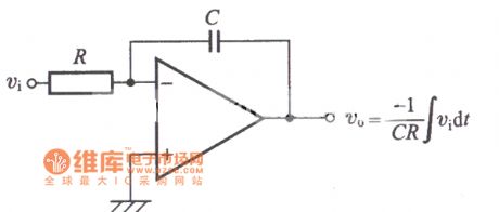
Integral circuit diagram shown as follow:
(View)
View full Circuit Diagram | Comments | Reading(1362)
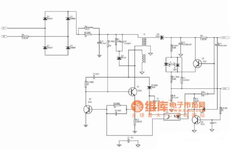
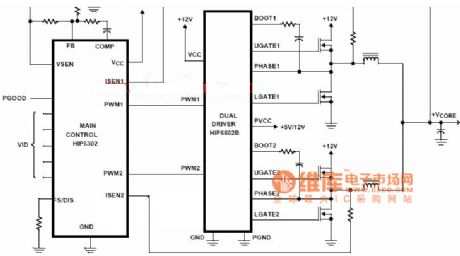
Synchronous rectifier adapter circuit 120W/12V/10A circuit diagram
Published:2014/3/20 21:03:00 Author:lynne | Keyword: Synchronous rectifier adapter circuit 120W/12V/10A circuit diagram,
Synchronous rectifier adapter circuit 120W/12V/10A circuit diagram shown as following:
(View)
View full Circuit Diagram | Comments | Reading(2207)
Small DC booster circuit diagram
Published:2014/3/19 21:09:00 Author:lynne | Keyword: Small DC booster circuit diagram,
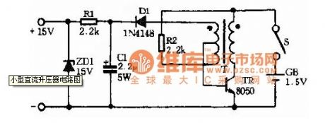
Small DC booster circuit diagram as shown:
(View)
View full Circuit Diagram | Comments | Reading(1787)
Dongfeng Peugeot Citroen Picasso 2.0L sedan electric mirrors Diagram
Published:2014/3/18 21:15:00 Author:lynne | Keyword: Dongfeng Peugeot Citroen Picasso 2.0L sedan electric mirrors Diagram,
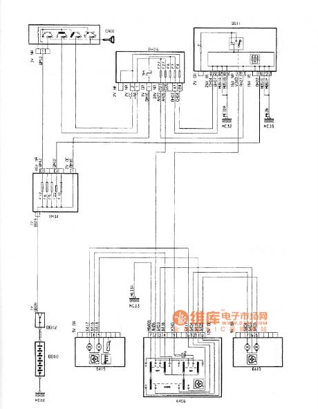
Dongfeng Peugeot Citroen Picasso 2.0L sedan electric mirrors Diagram shown as follow:
(View)
View full Circuit Diagram | Comments | Reading(1400)
Tl494 inverter circuit diagram
Published:2014/3/18 21:17:00 Author:lynne | Keyword: Tl494 inverter circuit diagram, Tl494
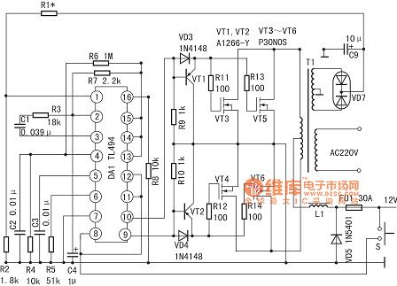
Tl494 inverter circuit diagram as shown:
(View)
View full Circuit Diagram | Comments | Reading(6974)
Sine wave inverter circuit diagram
Published:2014/3/17 21:29:00 Author:lynne | Keyword: Sine wave inverter circuit diagram, ICL7660, MAX1044
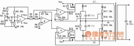
Existing inverter, well-sine wave output and output. High efficiency inverter square wave output, but are designed for the electrical sine wave power, the use is not always assured, although you can apply to many appliances, but some appliances do not apply, or electrical indicators up change. Sine wave output inverter no shortcomings in this area, but there is the disadvantage of low efficiency. Designed a highly efficient sine wave inverter, the circuit shown in Figure 1.
The circuit is powered by a 12V battery. First with a voltage doubler amplifier module times the pressure of supply. Can select ICL7660 or MAX1044. Op amp a 50Hz sine wave as a reference signal generated. 2 op amp as an inverter. 3 and op amp op amp as a comparator with hysteresis 4. In fact, the op amp 3 and switch a proportion of the switching power supply is constructed. Operational amplifier 4 and switch 2 also. Its switching frequency is unstable. In the op-amp output signal is positive phase, the op amp 3 and switch jobs. Then the output of op amp 2 is negative phase. Then the positive input of operational amplifier 4, the potential (fixed to 0) than the high potential of the negative input, the output of operational amplifier 4 is a constant, the switch is closed. In an op-amp output is negative phase, the opposite. This enables the two switches alternately work.
Below is a discussion about how the switch works. When the reference signal is less than the detection signal, that is the amplifier negative input terminal 3 or 4 signal is high a small value than the positive input signal, the comparator outputs 0, the switch opened, followed detection signal rapidly increased, when the detection signal higher than the reference value of a tiny signal, the comparator output 1, switch off. It should be noted here that, in the comparator circuit has a flip positive feedback, which is a hysteresis characteristic of the comparator. For example, under the reference signal is lower than the detection signal of the premise, as they continue to close the difference, at the moment they are equal, the reference signal detection signal immediately higher than a certain value. This certain value affect the switching frequency. The lower it is the greater frequency. Here choose it for the 0.1 ~ 0.2V.
C3, C4 role is to allow a high frequency current through the freewheeling switch, while the low-frequency impedance greater 50Hz signal. C5 by the equation: 50 = calculated. L is generally 70H, the production is best measured it. Thus C is about 0.15μ. The ratio of R4 and R3 should be strictly equal to 0.5, significantly larger waveform distortion, small start-up can not be, but rather a number of large, non-small. Maximum current switch is: I == 25A.
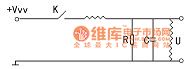
Click here for a more detailed discussion of selected values of L1, L2's. Equivalent to the load back to the input side of the transformer, the circuit of Figure 2.
Considering the switching frequency is much greater than 50Hz , the switch from on to off in the process , you can put a voltage transformer as a constant. The output of the power energy of the L : W = ∫ Uccdt = t
Ignore all the loss is not ideal , this energy should be equal to the load energy consumption . The average power of the formula : P == t
I hope when Ucc-U is close to a small value, the battery can be higher switching frequencies and to meet the requirements of the transformer. This a little value here take 0.5V, the frequency of taking 5kHz. When Ucc-U <0.5V, the switch will open a long time (which is relatively a ) . If you need the power of the maximum output power of 150W, then the load resistance is 322.7Ω, converted to the transformer input is : 0.48 Ω.
∴ instantaneous load power at this time is : P == 276W∴ P = × = 276∴ L = 2.2μH
L value can be seen in small disadvantage for the switch , and the output is clipping . You can increase the production of L values, but the maximum output power will be reduced. The best way to solve this problem is to use 16V power supply , the transformer is also used 8.5V (peak to 12V), and the peak for the reference signal of 12V , but this time the need to change the circuit . (View)
View full Circuit Diagram | Comments | Reading(2582)
AIC1896 integrated circuit diagram
Published:2014/3/16 21:13:00 Author:lynne | Keyword: AIC1896 integrated circuit diagram, AIC1896
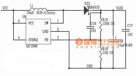
AIC1896 integrated circuit diagram shown as follow:
(View)
View full Circuit Diagram | Comments | Reading(1547)
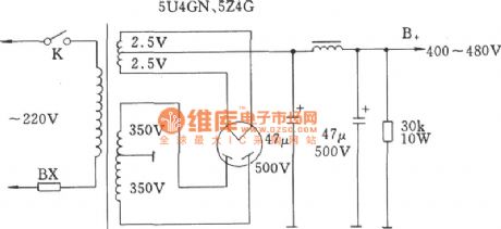
Tube full-wave rectified and filtered circuit Diagram
Published:2014/3/16 21:09:00 Author:lynne | Keyword: Tube full-wave rectified and filtered circuit Diagram,
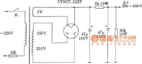

Tube full-wave rectified and filtered circuit Diagram shown as follow:
(View)
View full Circuit Diagram | Comments | Reading(1309)
PC, CPU overheat language warned circuit diagram
Published:2014/3/13 23:04:00 Author:lynne | Keyword: PC, CPU overheat language warned circuit diagram,

The circuit shown in FIG. It consists of a temperature sensor, temperature electronic switch circuit composed of sound and language. On hot summer season, PC's central processing unit CPU overheating often, the circuit VT1 die close to the CPU chip, radiator, once the CPU overheating, the circuit will issue a Notice that temperature cautioned statement, reminded officers to take measures to cool. (View)
View full Circuit Diagram | Comments | Reading(1495)
Motor overheating language newspaper called circuit diagram
Published:2014/3/13 22:59:00 Author:lynne | Keyword: Motor overheating language newspaper called circuit diagram,
The circuit shown in FIG. It consists of a temperature sensor, electronic circuit and the switching circuit composed of the language utterance. In the hot season, or when the temperature of the motor fails to run, often the motor overheating. The circuit can issue a beep, please note that the language of caution in the motor housing temperature alert duty personnel in order to avoid burn out the motor.
(View)
View full Circuit Diagram | Comments | Reading(1319)
Sound speed and cricket fans disgrace vocal control circuit diagrams
Published:2014/3/13 2:50:00 Author:lynne | Keyword: Sound speed and cricket fans disgrace vocal control circuit diagrams,
Circuit as shown, it includes acoustic sensor, audio amplifier, monostable trigger circuit, pulse counting/distribution circuit, thyristor speed regulation circuit, crickets sound circuit and ac step-down rectifier circuit, etc. Circuit using burst (such as punch, password) acoustic mode, three block wind speed can be control and stalling control, in the fan blowing at the same time, accompanied by filar silk cool meaning of crickets cry, strong anti-interference characteristics. (View)
View full Circuit Diagram | Comments | Reading(1690)
Tube high voltage circuit diagram
Published:2014/3/13 2:40:00 Author:lynne | Keyword: Tube high voltage circuit diagram,
Tube high voltage circuit diagram shown as follow:
(View)
View full Circuit Diagram | Comments | Reading(1355)
Battery level indicator circuit diagram
Published:2014/3/13 2:46:00 Author:lynne | Keyword: Battery level indicator circuit diagram,
Battery level indicator circuit diagram shown as follow:
(View)
View full Circuit Diagram | Comments | Reading(1590)
5G0401 acoustic synchronous flash with disco drum music circuit diagram
Published:2014/3/13 2:47:00 Author:lynne | Keyword: 5G0401 acoustic synchronous flash with disco drum music circuit diagram, 5G0401
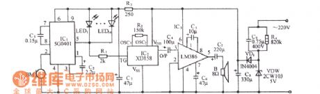
Circuit shown in Figure, which includes voice-activated flash circuit, drum music sound circuit and audio amplifier circuit and buck rectifier circuit. 5G0401 is the voice flash drive ASIC. (View)
View full Circuit Diagram | Comments | Reading(1424)
Hardware circuit ultrasonic range finder
Published:2014/3/6 20:53:00 Author:lynne | Keyword: Hardware circuit ultrasonic range finder,
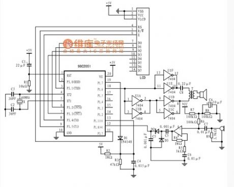


AT89C2051 by external pin P1.6 output pulse width is 250μs, the carrier is 10 pulses of 40kHz pulse group, added to the push-pull transformer primary form by upconverting promote emitted ultrasonic transducer. Simultaneously transmitted, P1.7 outputs a high level starts to charge the capacitor C4. The transmitting end toggles LOW HIGH divider C4 starts R2, R3, and the composition discharged to the negative output terminal of the comparator. Ultrasonic receiving transducer converts the received ultrasonic waves reflected by an obstacle to the amplifier for amplification, which is a high gain, low noise amplifier, the positive input of the detection signal will be amplified to detect the echo of the comparator end. The emission level of the output P1.7 can suppress the comparator flip, it can be suppressed so that the transmitter transmits the ultrasonic wave radiated to the error detection result of the receiver.
(View)
View full Circuit Diagram | Comments | Reading(2218)
Three-phase full-bridge application circuit diagram
Published:2014/3/6 20:55:00 Author:lynne | Keyword: Three-phase full-bridge application circuit diagram,
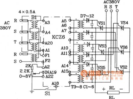
Pulse transformer can be tank-shaped Mn-Zn ferrite. Generally used U30 core or SEAR2: l pulse transformer. Three-phase full-bridge circuit diagram shown in Figure Application...
(View)
View full Circuit Diagram | Comments | Reading(1620)
845 motherboard circuit diagram
Published:2014/3/5 21:31:00 Author:lynne | Keyword: 845 motherboard circuit diagram
845 motherboard circuit diagram as shown:
(View)
View full Circuit Diagram | Comments | Reading(1332)
Santana 2000 anti-theft system circuit diagram
Published:2014/3/4 19:57:00 Author:lynne | Keyword: Santana 2000 anti-theft system circuit diagram,
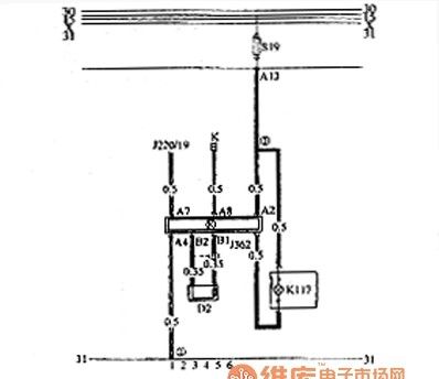
Santana 2000 anti-theft system circuit diagram shown in Fig.:
(View)
View full Circuit Diagram | Comments | Reading(1245)
Dongfeng Peugeot Citroen Picasso 2.0L sedan starting and charging system circuit diagram
Published:2014/3/3 20:21:00 Author:lynne | Keyword: Dongfeng Peugeot Citroen Picasso 2.0L sedan starting and charging system circuit diagram,
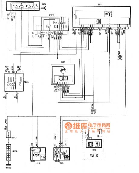
Dongfeng Peugeot Citroen Picasso 2.0L sedan starting and charging system circuit diagram shown in Fig.:
(View)
View full Circuit Diagram | Comments | Reading(1733)
Santana 2000GLs car air conditioning system circuit diagram
Published:2014/3/3 20:26:00 Author:lynne | Keyword: Santana 2000GLs car air conditioning system circuit diagram,
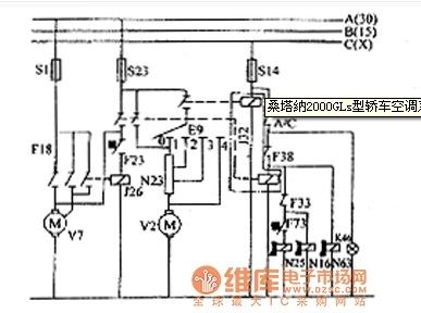
Santana 2000GLs car air conditioning system circuit diagram shown in Fig.:
(View)
View full Circuit Diagram | Comments | Reading(1411)
| Pages:5/471 1234567891011121314151617181920Under 20 |
Circuit Categories
power supply circuit
Amplifier Circuit
Basic Circuit
LED and Light Circuit
Sensor Circuit
Signal Processing
Electrical Equipment Circuit
Control Circuit
Remote Control Circuit
A/D-D/A Converter Circuit
Audio Circuit
Measuring and Test Circuit
Communication Circuit
Computer-Related Circuit
555 Circuit
Automotive Circuit
Repairing Circuit