
Basic Circuit
Index 375
A Simple Stabilized Voltage Circuit with Overcurrent Protection Function
Published:2011/7/7 22:46:00 Author:Michel | Keyword: Stabilized Voltage Circuit, Overcurrent Protection
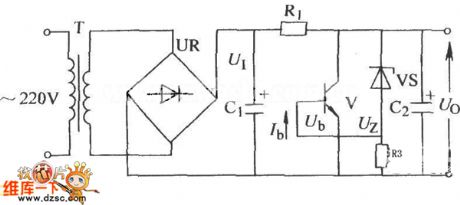
The stabilized voltage circuit with overcurrent protection function is shown as above.Welcome to download the circuit and this information is from www.dzsc.com. (View)
View full Circuit Diagram | Comments | Reading(544)
DS18B20 and 51 Single Chip AT89C2051 Interface Circuit
Published:2011/7/7 22:28:00 Author:Michel | Keyword: 51 Single Chip, Interface Circuit
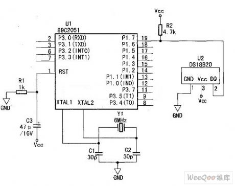
The DS18B20 and 51 single chip AT89C2051 interface circuit is shown as abvoe.The P1.7 mouth line of AT89C2051 is connected to pins 2 data side of DS18820 after being pulled.The pin 1 connects to low power port and pin 3 connects to +5V power supply end. (View)
View full Circuit Diagram | Comments | Reading(2765)
Contrast between SMT Telephone Processing Test Instruments 8960 and CMU200
Published:2011/6/25 8:04:00 Author:Michel | Keyword: Contrast, SMT Telephone, Processing Test Instruments
Part No.:8960/E5515CProduction Instructions
It is usedin largeproduction test of mobile phone production processing.
In the mass production of the mobile phone,test throughput and test pass rate are key problems considering of production.Agilent 8960 series 10 wireless communication test device provides the advantageous conditions of taking part in competition immediately for mobile phone producers.The 8960 series 10 test device provides rapid, accurate and repeatable,multiform ability, easy programming and flexible system structure.For phone manufacturers, , it is benificial to reducing test cost and increasing production. (View)
View full Circuit Diagram | Comments | Reading(876)
Basic Complementary Symmetry OTL Power Amplifier Circuit
Published:2011/6/25 7:19:00 Author:Michel | Keyword: Complementary, Symmetry, OTL Power, Amplifier Circuit
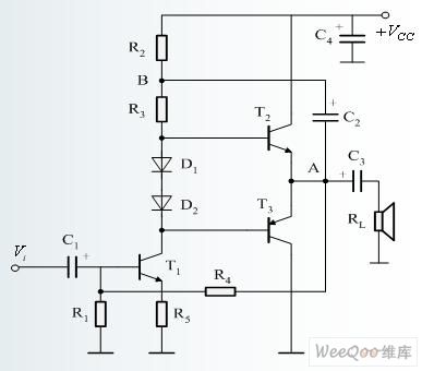
OTL is the English abbreviation of Output Transformer Less which means the transformer without output.OTL power amplifier is the power amplifier circuit that has not output coupling .OTL power amplifier mostly uses complementary and push-pull output level circuit.
The aboved picture is complementary symmetric OTL power amplifier circuit.T2 is a NPN power transistor,T3 is a PNP transistor and they constitutes complementary and push-pull output tube.T1 is voltage amplifier incentive tube.The signal is amplified in T1 after C1 coupling and its positive half cycle of signal which is generated by 1 collector makes T2 conduct.Its negative half cycle makes T3 conduct and the amplified signal outputs to speaker via capacitance C3.
(View)
View full Circuit Diagram | Comments | Reading(3302)
MAX16802 Typical Appliction Circuit
Published:2011/6/28 0:40:00 Author:Michel | Keyword: Typical, Appliction, Circuit
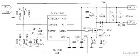
MAX16802 Typical Circuit is shown as above.Inspection flow resistance is compsoed of R9 and R10 in parallel form and voltage detection dividing resistor consists of R6 and R7.The MAX16802 current limit threshold is 291 mV, so we choose R9, R10, R6, and R7 can meet the calculated inductance peak current. Becuase of parasitic effect in the circuit,the resistance R7 value need proper adjustment to get the expecting current.
Picture:MAX16802 Typical Appliction Circuit (View)
View full Circuit Diagram | Comments | Reading(974)
Current / voltage conversion circuit composed of FET
Published:2011/7/6 5:08:00 Author:Lucas | Keyword: Current conversion , voltage conversion , FET
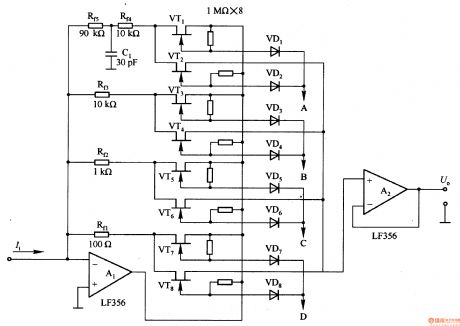
In the circuit, FET tube can switch feedback resistor Rf according to the size of the measured current to make output voltage be the specified value. The input signal is swicthed from DC signal to the lKHz AC signal with conversion accuracy in 0.1%. The accuracy of the feedback resistor and open-loop gain of Al affects the conversion accuracy. Al uses LF356, when the frequency is 1KHz, its open-loop gain is 3x1Ox1Ox1O to reach 0.1% conversion accuracy completely. A, B, C, D are switching control signal input ends.
(View)
View full Circuit Diagram | Comments | Reading(617)
Pulse width / voltage conversion circuit composed of TL082
Published:2011/7/5 8:16:00 Author:Lucas | Keyword: Pulse width , voltage conversion
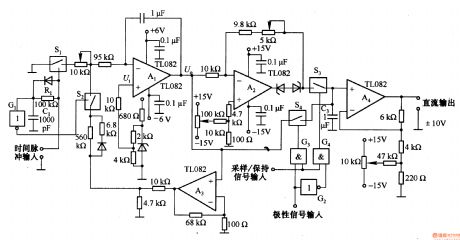
This is the pulse width (time) / voltage conversion circuit, according to the diagram component parameters, it can convert 0.1 S pulse width into 10V output voltage. When time pulse input end is added input conversion pulse, the analog switch Sl is disconnected, and S2 is connected, then Al integrator output is OV. This state has been maintained to be increased the input pulse. After added pulse, Sl is turned on and S2 is off, and the feedback loop is cut off, then Al makes integral on the reference voltage, and its output reduces in the negative direction and changes into low level at the end of integral. If the input pulse goes low, Sl is immediately disconnected.
(View)
View full Circuit Diagram | Comments | Reading(2926)
Precision full-wave rectifier circuit
Published:2011/7/6 7:32:00 Author:Lucas | Keyword: Precision , full-wave , rectifier circuit
Figure 1-37 (a) is the basic full-wave rectifier circuit. The operating frequency of actual circuit is limited. When the operating frequency is 1KHz, linear rectifier characteristic is very poor. So it could use the circuit shown in Figure 1-37 (b) to rectify high-frequency signals. The circuit is more complex, but the diode rectifier circuit uses the constant current drive mode with adding biasing on diode itself, so switching working recovery time can be greatly improved to be conducive to high-frequency rectifier. In the circuit, VTl, VT2 and VT5, VT6 constitute constant current source. (View)
View full Circuit Diagram | Comments | Reading(929)
Voltage / frequency conversion circuit composed of AD654
Published:2011/7/10 22:23:00 Author:Lucas | Keyword: Voltage conversion , frequency conversion
In the circuit shown as Figure 1-1 (a), AD820 is a high-impedance input voltage / current conversion circuit. In the case of neglecting DC error, AD820's 2pA bias current can make input impedance be megohms magnitude. AD654 is voltage / current conversion circuit with a single supply voltage, whcih could make operating current be about 3mA. During the voltage conversion period, VTl output current I (T) could incent AD654 to control the output frequency f. In the circuit, C1 selects 1nF capacitor.
(View)
View full Circuit Diagram | Comments | Reading(660)
TL496 switch regulator, main features and pin of DC-DC circuit and power supply monitor
Published:2011/7/10 2:04:00 Author:Lucas | Keyword: switch regulator, main features , pin , DC-DC circuit , power supply monitor
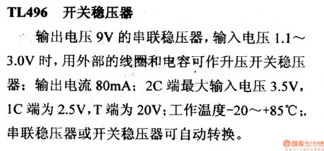
It is the series regulator with 9V output voltage, when input voltage is 1.1 ~ 3.0V, it uses an external coil and capacitoras step-up switching regulator; output current is 80mA; the maximum input voltage of 2C end is 3.5V; IC terminal is 2.5V, T end is 20V; Operating Temperature is -20 ~ +85 ℃; series regulator and switching regulator can be automatically converted.
(View)
View full Circuit Diagram | Comments | Reading(1750)
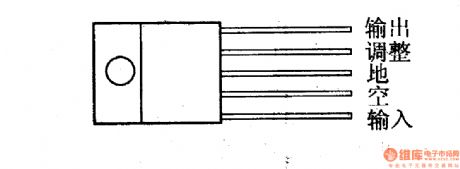
W4800 series of regulator, main features and pin of DC-DC circuit and power supply monitor
Published:2011/7/10 1:24:00 Author:Lucas | Keyword: regulator, main features , pin , DC-DC circuit , power supply monitor
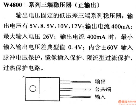
W4800 series of three-terminal regulator( positive output)
It is the three-terminal regulator with fixed output voltage; output voltage can be 5V, 8.5V, 10V, 12V; output current is 400MA; maximum input voltage is 26V; when output current is 400mA, the typically value of minimum dropout voltage is 0.4V; it contains ± 60V input pulse voltage protection, mirrored insert protection, current limiting type of overcurrent protection, overheat protection circuit.
(View)
View full Circuit Diagram | Comments | Reading(551)
W4920 series of regulator, main features and pin of DC-DC circuit and power supply monitor
Published:2011/7/10 1:41:00 Author:Lucas | Keyword: regulator, main features, pin , DC-DC circuit , power supply monitor
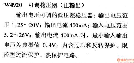
W4920adjustable regulator(positive output)
It is the three-terminal low dropout series of regulator with fixed output voltage; output voltage range is 1.25 ~ 20V; output current is 400mA; input voltage range is 5.2 ~ 26V; when output current is 400mA, the typical value of minimum dropout voltage is 0.4V; it includes overvoltage and reversal protection, current limiting type of overcurrent protection, thermal protection circuit.
(View)
View full Circuit Diagram | Comments | Reading(487)
W4960 switch regulator, main features and pin of DC-DC circuit and power supply monitor
Published:2011/7/10 1:58:00 Author:Lucas | Keyword: switch regulator, main features , pin , DC-DC circuit , power supply monitor
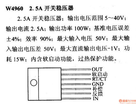
W4960 2.5A switch regulator
It is the 2.5A switching regulator; output voltage range is 5 ~ 40V; output current is 2.5A; output power is 100W; reference voltage error is ± 4%; efficiency is 90%; maximum input voltage is 50V;maximum difference between input and output voltage is 50V; the maximum DC output is -1V; power is 15W; it has the functions of soft start, thermal protection.
(View)
View full Circuit Diagram | Comments | Reading(550)
μA78G/79G series of regulator, main features and pin of DC-DC circuit and power supply monitor
Published:2011/7/9 8:38:00 Author:Lucas | Keyword: regulator , main features, pin , DC-DC circuit , power supply monitor
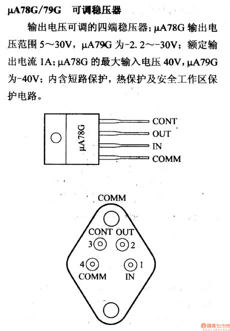
It is the four-terminal regulator with adjustable voltage; uA78G output voltage range is 5 ~ 30V, uA79G is -2.2 ~-30V; rated output current is 1A; the maximum input voltage of uA78G is 40V, uA79G is -40V; it includes short circuit protection, thermal protection and safe operating area protection circuit.
(View)
View full Circuit Diagram | Comments | Reading(1535)
The value circuit composed of DG201
Published:2011/7/6 8:47:00 Author:Lucas | Keyword: value circuit
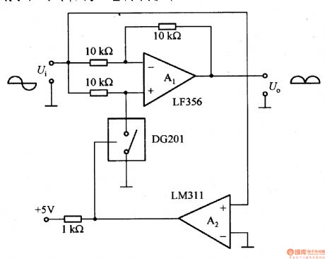
The circuit uses DG201 analog switch circuit and the zero-crossing comparator to control the polarity of the amplifier Al (in-phaseor inverting amplifier). When analog switch DG2O1 is off and the input signal is in positive half cycle, A2 output is in high level, and Al is a follower; when input signal is in negative half cycle, A2 output is in low level, then DGO1 is connected, and Al is equivalent to the inverting amplifier. In the circuit, A2 and DG2O1 is limited by the highest frequency, and the operating frequency is about lOkHz.
(View)
View full Circuit Diagram | Comments | Reading(1005)
TEX888H Communication Monolithic Micro-Computer Integrated Circuit Diagram
Published:2011/7/10 6:15:00 Author:Vicky | Keyword: Communication , Monolithic , Micro-Computer
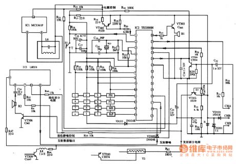
TEX888H is a communication monolithic micro-computer integrated circuit. It is usually used as mobile phone control circuit in cordless telephone.
Typical applied circuit diagram of mobile phone control which is composed of IC TEX888H is shown in picture 1.
Note: When dialing the number, failure in dialing is easy to happen to the mobile. Under such circumstance, check whether the keys are short-circuits or not first, whether the conductive rubber resistance becomes larger or not, and whether the inside mobile is affected with damp or not.
If password failure happens, you might emphasis on the check of the 18 pin of TEX888H and other exterior components. The possible reason of the malfunction can be judged by testing the dynamic or quiescent voltage of the pin. (View)
View full Circuit Diagram | Comments | Reading(3144)
200 V / 100 V voltage conversion circuit
Published:2011/7/6 9:07:00 Author:Lucas | Keyword: 200 V , 100 V, voltage conversion
Power transformer will wind primary winding into two groups of coils, and two groups of coils are used in parallel at 100V operation; groups of coils are used in series at 200V operation. When the converter uses half-bridge circuit, it needs the positive and negative power with the core of 0V. It is the best conversion method to directly drive the circuit by the power supply. It is the doubler rectifier circuit when the voltage is 100V, and it is the full-wave bridge rectifier circuit when the voltage is 200V. The flowing current of 100V is double of the 200v , and it uses double-pole-double-throw switch to switch the voltage, and it should be added 100v contacts. (View)
View full Circuit Diagram | Comments | Reading(487)
Current / voltage conversion circuit composed of LH0032
Published:2011/7/6 9:15:00 Author:Lucas | Keyword: Current conversion, voltage conversion
This is the Current / voltage conversion circuit with fast output voltage rising time, perfect frequency characteristics as the inverting amplifier, high-speed FET input operational amplifier. For making the output be consistent with the polarity of the input signal, Al output end is connected inverting amplifier A2. If you ignore the effects of stray capacitance, the output voltage rising time is about 3OμS, and it will switch the 50nA input current into lV output voltage. In the circuit, R2 is used to prevent the input oscillation; VTl and VT2 are connected as diodes, which is used for input protection of Al. (View)
View full Circuit Diagram | Comments | Reading(453)
Current / voltage conversion circuit composed of μA741
Published:2011/7/6 8:31:00 Author:Lucas | Keyword: Current conversion , voltage conversion
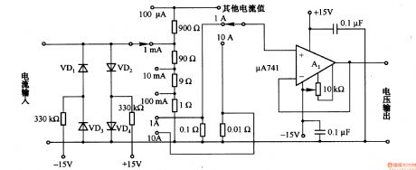
When it makes the current conversion with more than 100mA, you should pay attention on the wiring resistor. If the reference resistance is switched into lΩ or O.lΩ, the wiring cable resistance, base resistance of lead wire can not be ignored. For example, the base resistance is 0.lΩ, in order to control the conversion error in 0.1%, the total wiring resistance is 100μΩ. Also, you should pay attention to resistor heating problem. When the current is lA or more, the resistor will heat, then the temperature of resistor is increased. Due to the effect of temperature coefficient, the reference resistance change will cause conversion errors.
(View)
View full Circuit Diagram | Comments | Reading(772)
Current / voltage conversion circuit composed of LM301
Published:2011/7/6 8:09:00 Author:Lucas | Keyword: Current conversion , voltage conversion
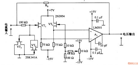
This is a low-input impedance conversion circuit with reference resistor RS being connected to the amplifier's feedback loop and input impedance in approximately zero, and the input current flows into Al's output end through Rs. The maximum switching current is decided by the op amp output current, and the maximum switching current of circuit is lOmA. When it needs to increase the current conversion, the output end of Al can be added current amplifier. VTl and VT2 use 2N3954 FET with the gate leakage current in 5OpA. If gate - drain voltage is reduced, the leakage current can be reduced to lOpA in the normal temperature. VT3 and VT4 are the protection FET (2SKl4lA).
(View)
View full Circuit Diagram | Comments | Reading(3488)
| Pages:375/471 At 20361362363364365366367368369370371372373374375376377378379380Under 20 |
Circuit Categories
power supply circuit
Amplifier Circuit
Basic Circuit
LED and Light Circuit
Sensor Circuit
Signal Processing
Electrical Equipment Circuit
Control Circuit
Remote Control Circuit
A/D-D/A Converter Circuit
Audio Circuit
Measuring and Test Circuit
Communication Circuit
Computer-Related Circuit
555 Circuit
Automotive Circuit
Repairing Circuit