
Relay Control
Index
Household automatic water supply device circuit principle diagram
Published:2013/12/30 20:56:00 Author: | Keyword: Household automatic water supply device circuit principle diagram,
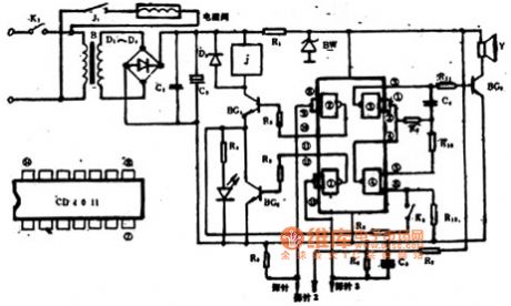
Household automatic water supply device circuit principle diagram
(View)
View full Circuit Diagram | Comments | Reading(1281)
The length of a probe based on circuit diagram of water vessel
Published:2013/12/30 20:44:00 Author: | Keyword: The length of a probe based on circuit diagram of water vessel,
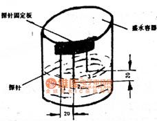
The length of a probe based on circuit diagram of water vessel
(View)
View full Circuit Diagram | Comments | Reading(892)
Household water supply printed circuit diagram
Published:2013/12/30 20:41:00 Author: | Keyword: Household water supply printed circuit diagram,
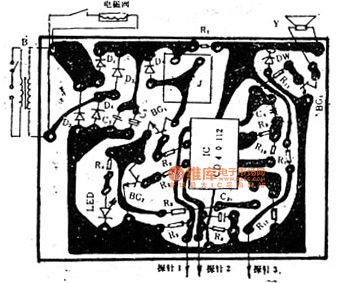
Household water supply printed circuit diagram
(View)
View full Circuit Diagram | Comments | Reading(944)
Control a Relay with Arduino – Tutorial #5
Published:2013/8/14 21:03:00 Author:lynne | Keyword: Control a Relay with Arduino , Tutorial #5
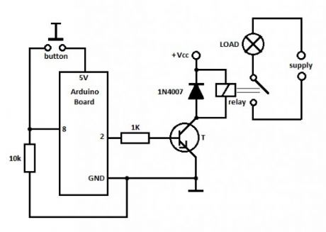
When the button is pressed the Arduino board will put pin 2 in HIGH state, meaning 5V on pin 2. This voltage is used to drive the transistor that will switch ON the relay and the load (in our case the fan) will be powered from the main power supply.
You cannot use the 5V from the USB to power up the transistor and the LOAD because the USB port usually delivers only 100mA, and this is not enough to switch the relay and the LOAD. That is why you must use an external power supply (Vcc) that is between 7 to 12 volts to power up the Arduino board and the transistor + relay. The load uses its own power supply, for instance if you use a light bulb then you might connect it to the 110/220V mains or any other power source.
(View)
View full Circuit Diagram | Comments | Reading(2008)
Power-Off Time Delay Relay
Published:2012/10/22 1:28:00 Author:muriel | Keyword: Power-Off Time, Delay Relay
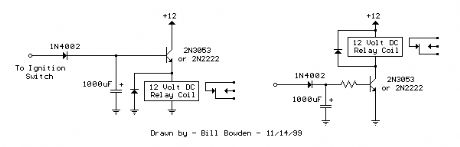
The two circuits below illustrate opening a relay contact a short time after the ignition or ligh switch is turned off. The capacitor is charged and the relay is closed when the voltage at the diode anode rises to +12 volts. The circuit on the left is a common collector or emitter follower and has the advantage of one less part since a resistor is not needed in series with the transistor base. However the voltage across the relay coil will be two diode drops less than the supply voltage, or about 11 volts for a 12.5 volt input. The common emitter configuration on the right offers the advantage of the full supply voltage across the load for most of the delay time, which makes the relay pull-in and drop-out voltages less of a concern but requires an extra resistor in series with transistor base. The common emitter (circuit on the right) is the better circuit since the series base resistor can be selected to obtain the desired delay time whereas the capacitor must be selected for the common collector (or an additional resistor used in parallel with the capacitor). The time delay for the common emitter will be approximately 3 time constants or 3*R*C. The capacitor/resistor values can be worked out from the relay coil current and transistor gain. For example a 120 ohm relay coil will draw 100 mA at 12 volts and assumming a transistor gain of 30, the base current will be 100/30 = 3 mA. The voltage across the resistor will be the supply voltage minus two diode drops or 12-1.4 = 10.6. The resistor value will be the voltage/current = 10.6/0.003 = 3533 or about 3.6K. The capacitor value for a 15 second delay will be 15/3R = 1327 uF. We can use a standard 1000 uF capacitor and increase the resistor proportionally to get 15 seconds. (View)
View full Circuit Diagram | Comments | Reading(1463)
Power-On Time Delay Relay
Published:2012/10/22 1:27:00 Author:muriel | Keyword: Power-On Time, Delay Relay
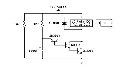
Here's a power-on time delay relay circuit that takes advantage of the emitter/base breakdown voltage of an ordinary bi-polar transistor. The reverse connected emitter/base junction of a 2N3904 transistor is used as an 8 volt zener diode which creates a higher turn-on voltage for the Darlington connected transistor pair. Most any bi-polar transistor may be used, but the zener voltage will vary from about 6 to 9 volts depending on the particular transistor used. Time delay is roughly 7 seconds using a 47K resistor and 100uF capacitor and can be reduced by reducing the R or C values. Longer delays can be obtained with a larger capacitor, the timing resistor probably shouldn't be increased past 47K. The circuit should work with most any 12 volt DC relay that has a coil resistance of 75 ohms or more. The 10K resistor connected across the supply provides a discharge path for the capacitor when power is turned off and is not needed if the power supply already has a bleeder resistor. (View)
View full Circuit Diagram | Comments | Reading(3519)
Light Operated Relay circuit
Published:2012/9/19 21:26:00 Author:Ecco | Keyword: Light Operated, Relay
This Light Sensitive Circuit can operate a Relay to switch on Lamps or any AC loads when it senses darkness. It is ideal to use as switch less Night lamps driver.
LDR is used as the light sensor. Its resistance is low about 100 ohms in bright light but increases to 10 meg or more in dark. Preset VR1 set the sensitivity of the LDR. During day time LDR conducts so that the gate of T1 will not get base bias. So that relay remains de energized. When the intensity of light reduces, LDR offers more resistance and more current passes to the base of T1 and it conducts. Relay then switch on the load. Adjust VR1 to trigger relay at the particular light level. LED indicates the activation of relay.
Light Operated Relay Circuit
?
8 Responses to “Light Operated Relay circuit”
Source: electroschematic.com
(View)
View full Circuit Diagram | Comments | Reading(1247)
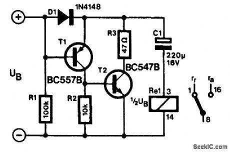
Temperature relay circuit
Published:2012/9/18 21:25:00 Author:Ecco | Keyword: Temperature relay
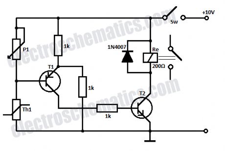
This simple temperature relay circuit can be used to signal a fire or setpoint for temperature monitoring function. You need to adjust P1 so that T1′s base voltage is 0.5V smaller than the emitter voltage at a temperature a little bit lower than the desired triggering (switching) temperature.If the temperature increases then T1 and T2 start conducting and the relay is closed (ON). If you want to use it as a cold relay or to signal an inferior temperature limit, then Th1 and P1 change places. After the relay is triggering you need to open switch S1 in order to stop the circuit. The nominal value of P1 must be choosed according to the used NTC thermistor and the switching temperature to be adjusted.
Temperature relay schematic
T1 can be BC557 and T2 BC547.
One Response to “Temperature relay circuit”
Source: electroschematics.com
(View)
View full Circuit Diagram | Comments | Reading(1763)
555 IC Hysteresis for Dark Activated Relay
Published:2012/9/3 3:06:00 Author:Ecco | Keyword: 555 IC , Hysteresis , Dark Activated Relay
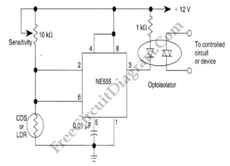
In the relay’s point of view, dark activated means the relay will be activated when the light intensity fall below a certain threshold. Without hysteresis, the relay will be activated and deactivated if the sensed brightness fall under or rise above a single point of darkness level. With hysteresis, the darkness level for activating and deactivating the relay will be different, and this solve the relay oscillation problem when the light intensity is swinging up and down around a single point of no hysteresis activation level.
We can employ the hysteresis of a 555 IC to improve the sensing of a drop in light, since the internal 555 circuit has 1/3 and 2/3 supply voltage thresholds. We have to use a LDR or CDS cell with aout 2 to 8 k resistance at desired light level. At the dark, the resistance of the LDR will rise and activate the relay if the voltage at pin 2 reach 2/3 of supply voltage (8V). After the relay is activated, more light is needed to make the LDR decrease its resistance until the voltage at pin 2 falls below 1/3 supply voltage (4V). (Source: freecircuitdiagram)
(View)
View full Circuit Diagram | Comments | Reading(2802)
Numeric control instrument of photoconductive control circuit diagram
Published:2011/8/2 1:09:00 Author:Ecco | Keyword: Numeric control instrument, photoconductive control
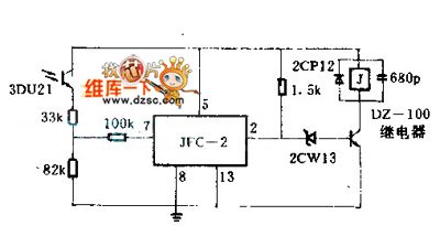
when a arbitrarily warping wire breaks, the light shield held by this warping wire will fall down, simultaneously, the light shield turns back the light that from the 3DU21 photosensitive tube, and the relay in the warping wire will be released, and that will make a parking by controlling its motor.
(View)
View full Circuit Diagram | Comments | Reading(845)
Liquid Level Controller (the 2nd)
Published:2011/8/12 4:52:00 Author:Felicity | Keyword: Liquid Level Controller
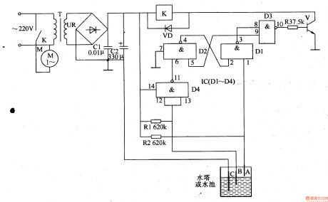
Work of the circuit
The circuit consists of power circuit and level detection and control circuit. (It is showed in picture 8-100.)
The power circuit consists of power transformer T, bridge rectifier UR and filter capacitor Cl, C2.
Level detection and control circuit consists of level electrode AC, four NAND gate IC IC (Dl-D4), the transistor V, resistors Rl-R3, relay K and diode VD.
220V AC voltage is bucked by T ,rectified by UR and filtered by C1, C2. It then supplies 12V voltage to relay K and IC. (View)
View full Circuit Diagram | Comments | Reading(1404)
FET Time Relay Circuit
Published:2011/9/3 10:01:00 Author:Zoey | Keyword: FET, Time Relay
FET Time Relay Circuit (View)
View full Circuit Diagram | Comments | Reading(1057)
Microwave turn-off delay device
Published:2011/8/14 22:52:00 Author:Ecco | Keyword: Microwave , turn-off delay device
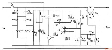
The microwave delay-off circuit is composed of the power supply circuit and delay control circuit, and it is shown in Figure 3-209. Power supply circuit consists of the nonstick button switch Sa, step-down capacitor Cl, resistor Rl, rectifier diodes VDl-VD4, voltage regulator diode VS and filter capacitor C2. Delay control circuit consists of op-amp integrated circuit IC, transistor V, relay K, delay capacitor C4, button switch Sb, current transformer TA, diodes VD5-VD7, resistor R7 and other components. Rl selects the 1/2W carbon film resistors; R2-R7 use the l/8W or 1/4W carbon film resistors.
(View)
View full Circuit Diagram | Comments | Reading(1569)
Solid-state relay basic wiring schematic diagram
Published:2011/8/8 0:21:00 Author:Sophia | Keyword: Solid-state relay, Wiring
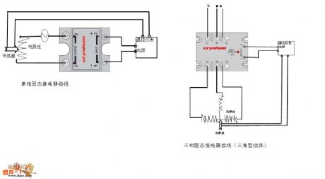
At present, solid-state relay has been applied to different industries. broadly speaking, solid-state relay includes several cpmtrol systems:
temperature control system, miniwatt motor control system, three-phrase electric machine regenerative control system, solenoid value control system, high frenquency system and so on. Butmany beginners and some engineers haven't engaged in these areas, so now I draw a simple wiring diagram for reference. (View)
View full Circuit Diagram | Comments | Reading(6775)
IR_RELAY_CIRCUIT
Published:2009/7/14 11:17:00 Author:May
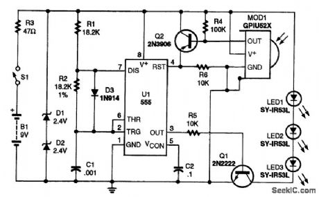
All IR is received by the module via an IR photodiode. The diode is operated in its reverse-bias current it permits depends on the intensity of the received infrared light. The fluctuations in the reverse-bias current are then amplified by a high-gain stage. The output of the amplifier is then limited by the next stage. The limiter chops the extreme highs and lows off the amplified signal, and the result is a quasi-digital pulse train. The simplified wave then passes through a bandwidth filter that has its center frequency at 40 kHz. At that point, the circuit has effectively retrieved the 40-kHz remote carrier. The reproduced carrier is then integrated. The next stage is an inverting Schmitt trigger. It will not go low unless the filter's output signal surpasses a certain amplitude, and it will not go high again until the signal drops below a certain minimum. Thus, the Schmitt trigger responds only to large changes in the filter's output (caused by bursts and pauses) and ignores small changes (caused by the 40-kHz carrier, to which the filter can't respond quickly). The Schmitt trigger's output is thus low when a 40-kHz burst is received, and high during pauses between bursts. The resulting waveform is an inverted version of the pulses that were modulated and transmitted by the remote. The oscillator circuit is based on a 555 timer. With D3, R2 is bypassed (or shorted out) while C1 is charging, but is in the current path during discharge. Therefore, with R1 and R2 made equal, the charge time equals the discharge time, yielding an output with a 50-percent duty cycle. Components R1, R2, and C1 (all precision, drift-free units) have been chosen to provide a 40-kHz output in this configuration. That output strobes the IR LEDs via Q1. The oscillator functions only when pin 4 of the 555 is high. Because that pin is connected to the inverter circuit, the oscillator functions when the inverter's input is low. The inverter's input is connected to MOD1's output, which goes low with each remote burst received. So overall, the circuit produces a 40-kHz IR burst when it receives one. (View)
View full Circuit Diagram | Comments | Reading(2081)
NONLATCHING_RELAY
Published:2009/7/9 21:03:00 Author:May
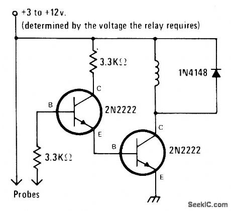
When liquid rises above level determined by positions of probes, circuit is triggered and relay, buzzer, or other indicator is energized. Alarm stops when liquid drops below preset level again. Use any operating voltage from 3 to 12 V that will actuate load employed.-J. A. Sandier, 9 Easy to Build Projects under $9, Modern Electronics, July 1978, p 53-56. (View)
View full Circuit Diagram | Comments | Reading(1251)
LOW_CONSUMPTION_MONOSTABLE_RELAY
Published:2009/7/9 0:44:00 Author:May
A monostable relay has two states: operative when a large enough current flows through its coil and quiescent when no current flows. A relay contact that assumes a certain position after the supply voltage has been switched on is required in many applications. Of course, many relays operate in that manner.However, most of these relays require an energizing current of 50 mA or more and that normally pre-cludes a battery supply. The circuit presented here, which uses a bistable relay, can solve that problem.The contact of a bistable relay normally remains in the position it is in after the supply is switched off. This circuit, however, makes the bistable relay behave like a monostable type, at a modest current.When the supply voltage is switched on, C1 charges via D1 and the relay coil. The current then flow-ing through the coil causes the relay contact to assume one of two positions. The forward drop across D1 ensures that the base of T1 (in this condition) is more positive than its emitter so that T1, and thus T2, is switched off.When the supply voltage is switched off, the emitter of T1 is connected to the positive terminal of C1, while the base is connected to the negative terminal of the capacitor via R1 and the relay coil. This results in T1, and thus T2, switching on so that C1 discharges via T4 and the relay. The current flows through the relay coil, then ftows in an opposite direction and this causes the contact to change oven The bistable relay thus behaves exactly as a monostable with the advantage, however, that the opera-tional current is determined by R1, which amounts to only 130 μA. To ensure reliable operation, the rating of the relay coil should be 65 to 75% of the supply voltage. In the prototype, a 9-V relay was used with a battery supply voltage of 12 V. (View)
View full Circuit Diagram | Comments | Reading(1969)
LATCHING_ac_SOLID_STATE_RELAY
Published:2009/7/9 0:41:00 Author:May
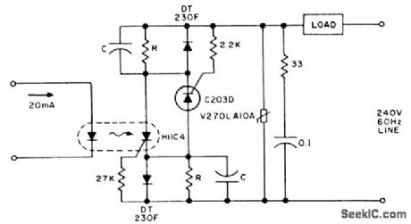
Latching is obtained by storing the gate trigger energy from the preceding half cycle in the capacitors. Power must be interrupted for more than one full cycle of the line to ensure turn-off. Resistor R and capacitor C are chosen to minimize dissipation, while assuring triggering of the respective SCRs for each cycle. A pulse of current, over 10 ms duration into the H11C4 IRED, ensures triggering the latching relay into conduction. (View)
View full Circuit Diagram | Comments | Reading(1453)
AC_RELAY
Published:2009/7/8 22:54:00 Author:May
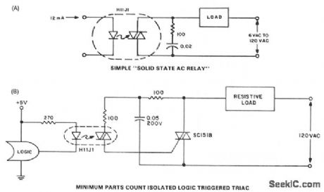
When zero voltage switching is not required, methods of providing this function are illustrated. The lowest parts count version of a solid-state relay is an optoisolator, the triac driver H11J. Unfortunately, the ability of the H11J to drive a load on a 60-Hz line is severely limited by its power dissipation and the dynamic characteristics of the detector. These factors limit applications to 30 - 50 mA resistive loads on 120 Vac, and slightly higher values at lower voltages. These values are compatible with neon lamp drive, pilot, and indicator incandescent bulbs; low voltage control circuits, such as furnace and bell circuits, if dV/dt are sufficient; but less than benign loads require a discrete triac.
The H11J1 triac trigger optocoupler potentially allows a simple power switching circuit utilizing only the triac, a resistor, and the optocoupler. This configuration will be sensitive to high values of dV/dt and noise on normal power-line voltages, leading to the need for the configuration shown in Fig. 67-14B, where the triac snubber acts as a filter for line voltage to the optocoupler.
Since the snubber is not usually used for resistive loads, the cost effectiveness of the circuit is compromised somewhat. Even with this disadvantage, the labor, board space, and inventory of parts savings of this circuit prove it cost-optimized for isolated logic control of power-line switching. In applications where transient voltages on the power line are prevalent, provisions should be made to protect the H11J1 from breakover triggering. (View)
View full Circuit Diagram | Comments | Reading(1381)
DC_LATCHING_RELAY
Published:2009/7/8 22:53:00 Author:May
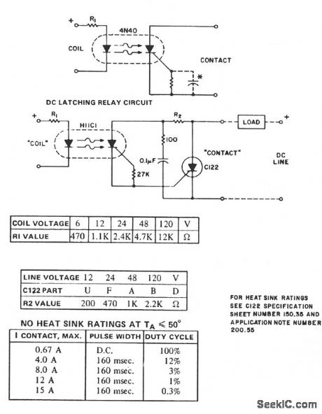

The H11C supplies the dc latching relay function and reverse polarity blocking, for currents up to 300 mA, depending on ambient temperature. For dc use, the gate cathode resistor can be supplemented by a capacitor to minimize transient and dV/dt sensitivity. For pulsating dc operation, the capacitor value must be designated to either retrigger the SCR at the application of the next pulse or prevent retriggering at the next power pulse. If not, random or undesired operation might occur. For higher current contacts, the H11C can be used to trigger an SCR capable of handling the current, as illustrated.
(View)
View full Circuit Diagram | Comments | Reading(1227)
| Pages:1/8 12345678 |
Circuit Categories
power supply circuit
Amplifier Circuit
Basic Circuit
LED and Light Circuit
Sensor Circuit
Signal Processing
Electrical Equipment Circuit
Control Circuit
Remote Control Circuit
A/D-D/A Converter Circuit
Audio Circuit
Measuring and Test Circuit
Communication Circuit
Computer-Related Circuit
555 Circuit
Automotive Circuit
Repairing Circuit