
Index 166
DARKROOM_TIMER
Published:2009/6/24 23:13:00 Author:May
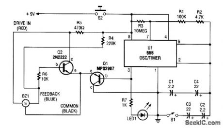
The electronic darkroom timer is built around a 555 oscillator/timer, a pair of general-purpose transistors, a buzzer, and an LED. The 555 (U1) is configured as an astable multivibrator (free-rututing oscillator). The frequency of the oscillator is determined by the values R1 through R3 and C1 through C4.
Switch S1 is used to divide the capacitor network to vary the time interval between beeps; when S1 is closed, the circuit beeps at intervals of 30 seconds. With S1 closed, it beeps at 15-second intervals.
When power is applied to the circuit (by closing switch S2), the output of U1 at pin 3 is initially high. That high is applied to the base of transistor Q1 (an MPS2907 general-purpose pnp device), keeping it turned off. That high is also applied to the anode of LED1 (which is used as a power on indicator) through resistor R7, turning it on.
Timing capacitors C1 through C5 begin to charge through timing resistors R1 through R3. dc voltage is applied to BZ1's driver input through R5 and to its feedback terminal (through R4), which is also connected to Q2's base terminal. The V+ voltage that applied to Q2's base causes it to turn on, tying BZ1's common terminal high.
When the timing capacitors are sufficiently charged, a trigger pulse is applied to pin 2 (the trigger input) of U2, causing U1's output to momentarily go low. This causes LED1 to go out and tran-sistor Q1 to turn on. That, in turn, grounds the common lead of buzzer BZ1, causing BZ1 to sound. Afterward, the output of U1 returns to the high state, turning off Q1, and turning on LED1, until another time interval has elapsed and the process is repeated.
The circuit is powered by a 9-Vac adapter, which plugs into a standard 117-V household outlet. Because the circuit draws only about 10 to 15 mA, a 9-V alkaline transistor-radio-battery can also be used to power the circuit. (View)
View full Circuit Diagram | Comments | Reading(0)
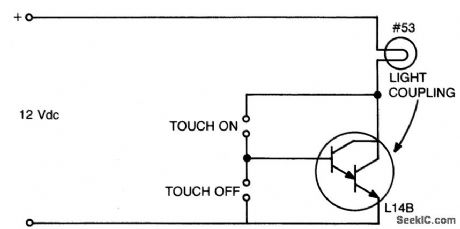
LATCHING,DOUBLE_BUTTON_TOUCH_SWITCH
Published:2009/6/24 23:11:00 Author:May
View full Circuit Diagram | Comments | Reading(0)
CMOS_TOUCH_SWITCH
Published:2009/6/24 23:10:00 Author:May
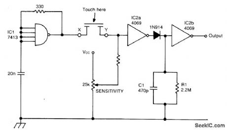
This touch switch does not rely on mains hum for switching. It can be used with battery powered circuits. Schmitt trigger IC1 forms a I 100 kHz oscillator and IC2a which is biased into the linear region, amplifies the output and charges C1 via the diode. IC2b acts as a level detector. When the sensor is touched, the os-cillator signal is severely attenuated which causes C1 to discharge and IC2b to change state. (View)
View full Circuit Diagram | Comments | Reading(0)
CAPACITANCE_OPERATED_ALARM_TO_FOIL_PURSE_SNATCHERS
Published:2009/6/24 23:01:00 Author:May
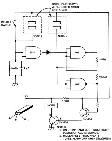
Aslong as touch plates (1) are touched together,the alarm is off. If not held for about 30 seconds,the alarm goes off. The circuit can be disabled with switch or by touching the plates (2),The alarm is battery operated by a bicycle horn. (View)
View full Circuit Diagram | Comments | Reading(0)
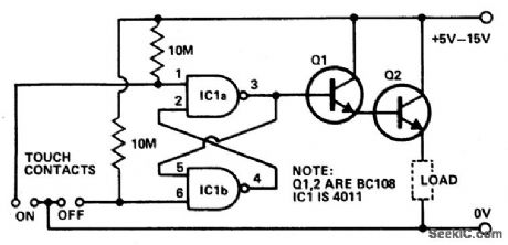
MOMENTARY_OPERATION_TOUCH_SWITCH
Published:2009/6/24 22:59:00 Author:May
View full Circuit Diagram | Comments | Reading(819)
IC_CARRIER_CURRENT_TRANSMITTER
Published:2009/6/24 23:29:00 Author:Jessie

View full Circuit Diagram | Comments | Reading(1422)
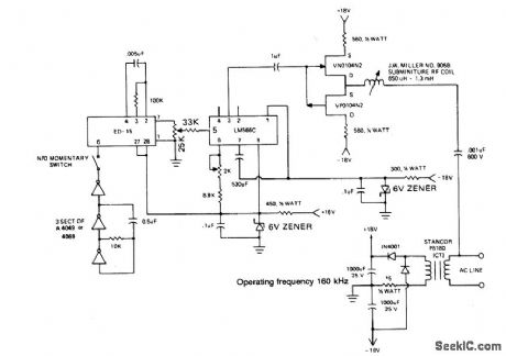
CARRIER_CURRENT_TRANSMITTER_1
Published:2009/6/24 23:25:00 Author:Jessie
View full Circuit Diagram | Comments | Reading(1386)
CARRIER_CURRENT_TRANSMITTER
Published:2009/6/24 23:24:00 Author:Jessie
View full Circuit Diagram | Comments | Reading(1768)
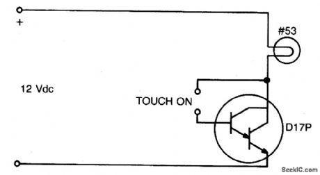
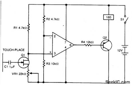
LOW_CURRENT_TOUCH_SWITCH
Published:2009/6/24 22:57:00 Author:May


Touching the on contacts with a finger brings pin 3 high, pair and supplying power to the load (transistor radio etc). transistor, and Q2 is chosen for the current required by the turning on the Darlington Q1 must be a high gain load circuit. (View)
View full Circuit Diagram | Comments | Reading(698)
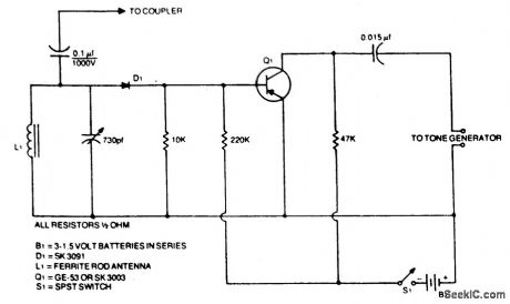
CARRIER_CURRENT_RECEIVER
Published:2009/6/24 23:21:00 Author:Jessie
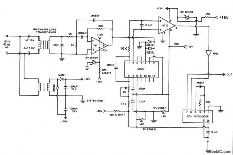
160 kHz transformer consists of a 18 x 11mm ungapped pot core (Siemens, Ferrocube, etc.), itilizing magnerics incorporated type F material wond woth 80 1/2 turns of No.35 sire for the secondary and 5 1/2 turns for the primary. This gives a turns ratio fo approximately 15 to 1. (View)
View full Circuit Diagram | Comments | Reading(3247)
TOUCH_SENSITIVE_SWITCH
Published:2009/6/24 22:56:00 Author:May
A high impedance input is provided by Q1, a general purpose field effect transistor. 741 op amp is used as a sensitive voltage level switch which in turn operates the current Q2, a medium current PNP bipolar transistor, thereby energizing the relay which can be used to control equipment, alarms, etc. (View)
View full Circuit Diagram | Comments | Reading(1965)
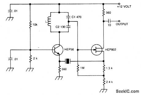
OVERTONE_OSCILLATOR_WITH_CRYSTAL_SWITCHING
Published:2009/6/24 23:18:00 Author:Jessie
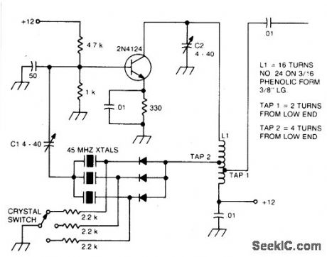
Circuit Notes
The large inductive phase shift of L1 is compensated for by C1. Overtone crystals have very narrow bandwidth; therefore, the trimmer has a smaller effect than for fundamental-mode operation. (View)
View full Circuit Diagram | Comments | Reading(1293)
CAPACITANCE_RELAY
Published:2009/6/24 22:54:00 Author:May
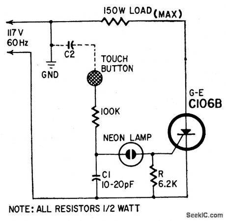
Capacitor C1 and body capacitance (C2) of the operator form the voltage divider from the hot side of the ac line to ground. The voltage across C1 is determined by the ratio of C1 to C2. The higher voltage is developed across the smaller capacitor. When no one is close to the touch button, C2 is smaller than C1. When a hand is brought close to the button, C2 is many times larger than C1 and the major portion of the line voltage appears across C1. This vol-tage fires the neon lamp, C1 and C2 discharge through the SCR gate, causing it to trigger and pass current through the load. The sensitivity of the circuit depends on the area of the touch plate. When the area is large enough, the cir-cuit responds to the proximity of an object rather than to touch. C1 may be made variable so sensitivity can be adjusted. (View)
View full Circuit Diagram | Comments | Reading(965)
CRYSTAL_CONTROLLED_BUTLER_OSCILLATOR
Published:2009/6/24 23:13:00 Author:Jessie
Circuit NotcsA typical Butler oscillator (20-100 MHz) uses an FET in the second stage; the circuit is not reliable with two bipolars. Sometimes two FETs are used. Frequency is determined by LC values. (View)
View full Circuit Diagram | Comments | Reading(1791)
LATCHING,DOUBLE_BUTTON_TOUCH_SWITCH
Published:2009/6/24 23:11:00 Author:Jessie
View full Circuit Diagram | Comments | Reading(1123)
CMOS_TOUCH_SWITCH
Published:2009/6/24 23:10:00 Author:Jessie
This touch switch does not rely on mains hum for switching. It can be used with battery powered circuits. Schmitt trigger IC1 forms a I 100 kHz oscillator and IC2a which is biased into the linear region, amplifies the output and charges C1 via the diode. IC2b acts as a level detector. When the sensor is touched, the os-cillator signal is severely attenuated which causes C1 to discharge and IC2b to change state. (View)
View full Circuit Diagram | Comments | Reading(1957)
FIFTH_OVERTONE_OSCILLATOR
Published:2009/6/24 23:06:00 Author:Jessie
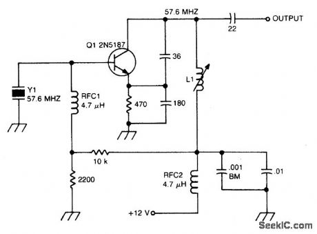
Circuit NotesThis circuit isolates the crystal from the dc base supply with an rf choke for better starting characteristics. (View)
View full Circuit Diagram | Comments | Reading(1271)
FINGER_TOUCH_OR_CONTACT_SWITCH
Published:2009/6/24 23:05:00 Author:Jessie
View full Circuit Diagram | Comments | Reading(687)
SELF_BIASED_PROXIMITY_SENSOR_WORKS_ON_DETECTED_CHANGING_FIELD
Published:2009/6/24 23:03:00 Author:Jessie
View full Circuit Diagram | Comments | Reading(0)
50_MHz_150_MHz_OVERTONE_OSCILLATOR
Published:2009/6/24 23:02:00 Author:Jessie
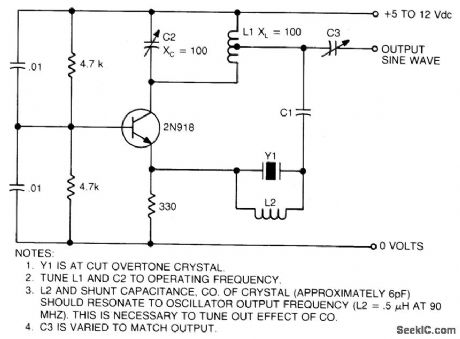
View full Circuit Diagram | Comments | Reading(1130)
| Pages:166/312 At 20161162163164165166167168169170171172173174175176177178179180Under 20 |
Circuit Categories
power supply circuit
Amplifier Circuit
Basic Circuit
LED and Light Circuit
Sensor Circuit
Signal Processing
Electrical Equipment Circuit
Control Circuit
Remote Control Circuit
A/D-D/A Converter Circuit
Audio Circuit
Measuring and Test Circuit
Communication Circuit
Computer-Related Circuit
555 Circuit
Automotive Circuit
Repairing Circuit