
TV Circuit
Index
New degaussing principle circuit
Published:2011/11/11 2:03:00 Author:May | Keyword: degaussing principle
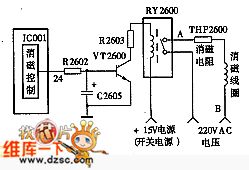
Because the voltage on capacitor C2605 can not mutation, this high level signal thorugh R2602 resistor first charges to C2605, because charging time constant is very big, the high level potential build at C2605 lags to the start time. Whenit isin starting process, capacitor finishes charging, VT2600 tube's base is inhigh level and breakover, relay RY2600 coil generates current access, its touching point is cut-off, degaussing circuit power source ( AC) accessis cut, thereby itfinishes the cut-off movement of degaussing circuit.
diagram 3: TV new type degaussing circuit
After shutdown, IC001's pin changes to low level, capacitor C2605discharges through VT2600's b-e junctions and IC001 internal concerning circuit, and the discharging time constant is also very high, so VT2600 tube changes to cutoff state after delay period of time, relay RY2600 again recovers to normal close state for degaussing next time.
(View)
View full Circuit Diagram | Comments | Reading(1561)
TV lightning protection circuit
Published:2011/10/26 22:14:00 Author:May | Keyword: TV lightning protection
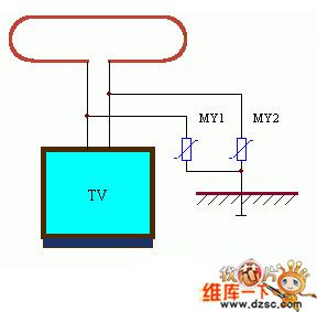
The application circuit of this set is shown in the picture. Watching TV on in thunderstorms, the thunderbolt can scurry into TV and damage it through two ways; one is through outdoor television antenna; the other is through TV power line. The former often damages radio-frequency head, the latter often damages TV power supply circuit and line-field output circuit. Adding voltage dependent resistor on outdoor antenna can avoidthe consequence, and itrequires voltage dependent resistor MY to beconnected with ground directly. Protective power supply part application circuit's connectioncan be seen in the picture. They general protect induced lightning, if it meets the direct lightening, because of thedirect lightening's huge current and extreme high voltage, voltage dependent resistor cannot do anything about it, so we should place lightning conductor around outdoor antenna, the position of outdoor antenna should bein the protected areas.
(View)
View full Circuit Diagram | Comments | Reading(2105)
Video Preamplified Circuit Diagram
Published:2011/9/14 0:26:00 Author:Zoey | Keyword: Video Preamplified
SID2141X is a kind of video preamplifier IC and it is widely used in a variety of domestic and imported color monitors.
The SD2141X integrated circuit contains a three-color signal processing circuit, a three-color gain control circuit, and a blanking signal processing circuit,tec. The circuit uses 20-pin dual in-line package, and the circuits have been used in LGCB56lBN color monitors, its foot arch function and data of the integrated circuit have been listed in Table 1. (View)
View full Circuit Diagram | Comments | Reading(1186)
Application Circuit of LCD TV Power
Published:2011/9/3 10:19:00 Author:Zoey | Keyword: Application Circuit, LCD TV Power
PLC810PG group and LLC lineless controller integrate with high pressure half-bridge driver. Picture 1 shows the circuit of PLC810PC power supply configuration.
PFC of PLC810PG uses a general continuous current mode that does not have to refer to sine signal, in this way, costs of the system and exterior accessories are reduced.
DC-DC controller drives the LLC resonance topologies.
Dead band time of LLC switch in PLC810PG can be adjusted by an exterior resistance.
PFC converter’s frequency is limited in LLC to reduce the interference of noise and electromagnetism.
This design also refers to elementary exception handles of PFC and LLC. Dynamic adjustment can be achieved by consulting phase proportion of LLC to PFC.
(View)
View full Circuit Diagram | Comments | Reading(1225)
SID2141X Video Preamplified Circuit Diagram
Published:2011/9/3 21:28:00 Author:Zoey | Keyword: Video Preamplified
SID2141X is a kind of video preamplifier ICand it iswidely used in a variety of domestic and imported color monitors. The SD2141X integrated circuit contains a three-color signal processing circuit, a three-color gain control circuit, and ablanking signal processing circuit,tec. Thecircuit uses20-pin dual in-line package, and the circuits have been used in LGCB56lBN color monitors,its foot arch function and dataof the integrated circuit have been listed in Table 1. (View)
View full Circuit Diagram | Comments | Reading(1000)
ATV_LINE_SAMPLER
Published:2009/7/12 23:14:00 Author:May

This device can be used to recover demodulated video from the output of an ATV transmitter. A small sample of the signal on the antenna feeder is tapped off and detected, and the resultant video is fed to an emitter follower. C1 is chosen for 1 V p-p under normal transmit conditions. This circuit was intended for 440-MHz AM TV signals. It will not work for FM or for 900-MHz or 1300-MHz signals. A striplike directional coupler can be used to sample the RF line without introducing an im-pedance bump.
(View)
View full Circuit Diagram | Comments | Reading(1395)
SIMPLE_MONOCHROME_TV_PATTERN_GENERATOR
Published:2009/7/11 3:14:00 Author:May
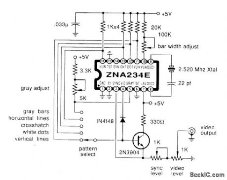
Using a Plessey ZNA234E IC, this generator produces sync, blankin gray bars lines, dots and crosshatch patteflls. (View)
View full Circuit Diagram | Comments | Reading(2114)
TV_LINE_PULSE_EXTRACTOR
Published:2009/7/11 2:38:00 Author:May
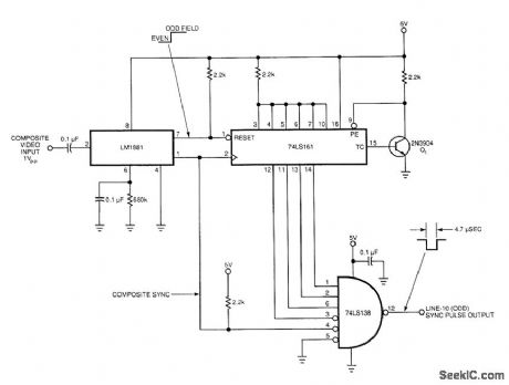
This circuit uses a sync-generator chip, a counter, and a decoder to detect the horizontal sync pulse that occurs at the bGginning of line 10 in field 1 of an NTSC television picture. You can use this circuit to compare the time delay between sync signals at various locations, and to determine and correct for any drift between the two master clocks.The output of the LM1881 sync separator is the key to detecting line 10; the odd/even line goes high on the leading edge of the first equalizing pulse in the middle of line 4. Thus, you can use this knowledge to find virtually any other line in the field. This particular circuit locates line 10 of field one. The circuit resets the 74LS161 counter until the odd/even line goes high. Then, 74LS161 counts the positive transitions of the sync signal. After 11 positive transitions, the sync pulse drives pin 4 of the 74LS138 decoder low, and the line-10 sync pulse appears at pin 12 of the decoder. (The circuit counts to 11, as opposed to the 6 you might expect-because the composite sync signal contains more than 1 pulse per line). The counter remains in its maximum-count state until the sync separator causes a reset because Q1 feeds the inverted terminal-count output back to the parallel-enable input. (View)
View full Circuit Diagram | Comments | Reading(1984)
COLOR_FOR_TV_TYPEWRITER
Published:2009/7/10 22:19:00 Author:May

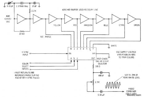
Uses 3.579545-MHz crystal osdllator to drive string of CMOS buffers forming digital delay line. Output delays caused by propagation times in each buffer can be used directly or can be trimmed to specific colors by varying supply voltage. Reference phase and delayed color outputs go to 1-of-8 data selector whose output is determined by code presented digitally to its three color select Iines. Selector drive Iogic must retum to 000 (reference phase) immediately before, during, and for at least several microseconds after each.horizontal sync pulse so set can lock and hold on reference color burst. Sine-wave output chrominance signal is cut down to about one-fourth of maximum video white level.-D. Lancaster, TV Typewriter Cookbook, Howard W Sams, Indianapolis, IN, 1976, p 205-206. (View)
View full Circuit Diagram | Comments | Reading(1872)
TV_INTERFACE_FOR_TYPEWRITER
Published:2009/7/10 22:18:00 Author:May

Video input circuitfor black and white transistor TV receiver permits feeding video output of TV typewriter to video driver in set, for producing character or DRIVER game display on TV screen. Use of direct coulpling eliminates shading effect or changes in background level as characters are added.Diodes provide 1.2-V offset in positive direction so in absence of video the video driver is biased to blacker-than-black sync level of 1.2 V. With white video input of 2 V, driver is biased to usual 3.2 V of white level. Hot-chassis TV sets can present shock hazard.-D, Lancaster, TV Typewriter Cookbook, Howard W. Sams, Indianapolis, IN, 1976, p 190. (View)
View full Circuit Diagram | Comments | Reading(1259)
TV_TRANSMITTER_1
Published:2009/7/8 20:58:00 Author:May
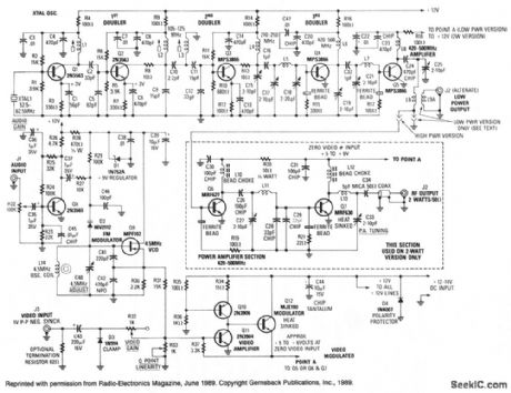
The video-link transmitter accepts color and B/W video, and audio inputs from VCRs, camcorders, small TV cameras, and microphones. The unit runs on a nominal 12 Vdc and draws 100 mA in the lowpower version, or 500 mA in the 2-W version. The kit is available from North Country Radio, P.O. Box 53, Wykagyl Station, NY 10804. (View)
View full Circuit Diagram | Comments | Reading(3391)
TV_TRANSMITTER
Published:2009/7/8 4:58:00 Author:May
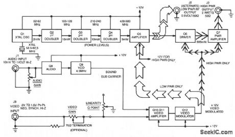
This transmitter is capable of two levels of rf power. For low-power wireless video, like in a house or office, where simultaneous monitoring of program material is desirable without cumbersome hookups, 1-30 mW is available. For longer ranges up to several miles, as in amateur (ham) TV, security, and surveillance purposes, 2 W into a 50-Ω oad is available. (View)
View full Circuit Diagram | Comments | Reading(88)
UPPERCASE_DRIVE_FOR_TV_GRAPHICS
Published:2009/7/5 22:25:00 Author:May
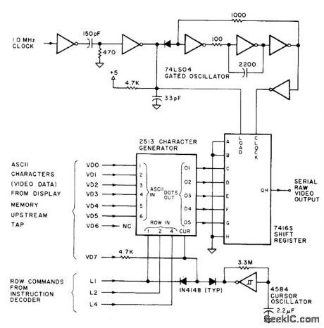
Alphameric data-to-video converter using 2513 character generator accepts ASCII words from microprocessor memory and three line commands from instruction decoder. Five dots are outputted simultaneously, corresponding to one row on 5 x 7 dot-matrix character. 7416S eight-input one-output shift register converts dots into serial output video. Input repeats to generate all seven dot rows in row of characters. Shift register is driven by high-frequency timing circuit that delivers LOAD pulse once each microsecond along with CLOCK output running continuously at desired dot rate. Optional cursor uses 4584 5-Hz oscillator for cursor winking rate. If ASCII input bit 8 is high, cursor input goes high and output is white line on leads 01 through 05. Right diode mades this line blink, while Ieft diode allows winking cursors only during valid character times.-D. Lancaster, TVT Hardware Design. Kilobaud, Jan. 1978, p 64-68. (View)
View full Circuit Diagram | Comments | Reading(1747)
STEREO_TV_DECODER
Published:2009/7/1 20:28:00 Author:May
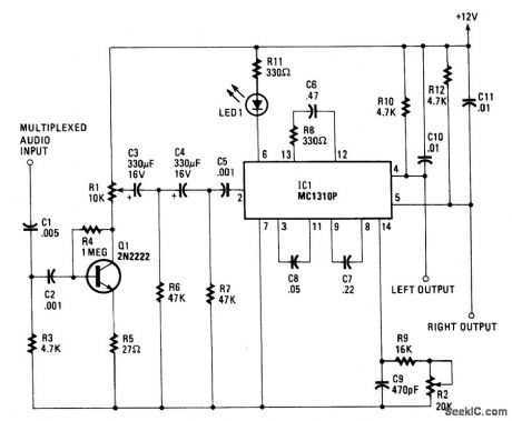
The composite input signal is preamplified by transistor Q1 and is then coupled to the high-pass filter composed of C3, C4, R6, and R7. The filtered audio is then passed to IC1, an MC1310P Coilless Stereo Demodulator. That IC is normally used to demodulate broadcast-band FM signals, but by changing the frequency of its on-board VCO (Voltage Controlled Oscillator) slightly (from 19 kHz to 15.734 kHz), we can use that IC to detect stereo-TV signals. A block diagram of the MC1310P is shown in Fig.22-5. Notice that the components connected to pin 14 control the VCO's frequency, hence the pilot-detect and carrier frequencies. For use in an FM receiver, the VCO would run at four times the 19 kHz pilot frequency (76 kHz), but for our application, it will run at four times the 15.734 kHz pilot frequency of stereo TV, or 62.936 kHz. The MC1310P divides the master VCO signal by two in order to supply the 31.468 kHz carrier that is used to detect the L - R audio signal. The L - R signal undergoes normal FM detection, and at that point we've got two audio signals: L + R and L - R. The decoder block in the IC performs the addition and subtraction to produce the separate left and right signals. R10and C10 form a de-emphasis network that compensates for the 75μs pre-emphasis that the left channel underwent; R12 and C11 perform the same function for the right channel. (View)
View full Circuit Diagram | Comments | Reading(0)
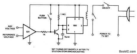
AUTOMATIC_TURN_OFF_FOR_TV_SET
Published:2009/6/29 3:51:00 Author:May
View full Circuit Diagram | Comments | Reading(732)
TV_MODULATOR_USING_A_MOTOROLA_MC1374
Published:2009/6/25 22:13:00 Author:May
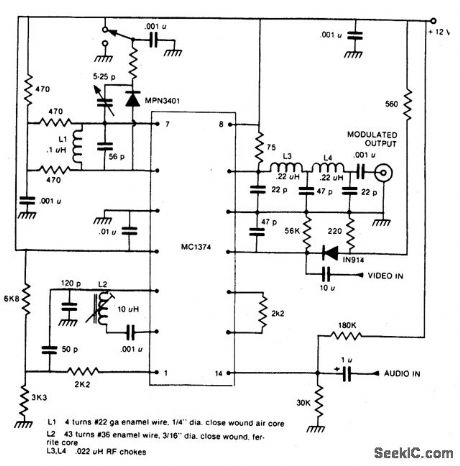
This one-chip modulator requires some outboard circuitry and a shielded box. (View)
View full Circuit Diagram | Comments | Reading(1248)
TV_MODULATOR
Published:2009/6/25 21:53:00 Author:May
The FM oscillator/modulator is a voltage-controlled oscillator, which exhibits a nearly linear output frequency versus input voltage characteristic for a wide deviation. It provides a good FM source with a few inexpensive external parts. It has a frequency range of 1.4 to 14 MHz and can typically produce a ±25 kHz modulated 4.5 MHz signal with about 0.6% total harmonic distortion. (View)
View full Circuit Diagram | Comments | Reading(0)
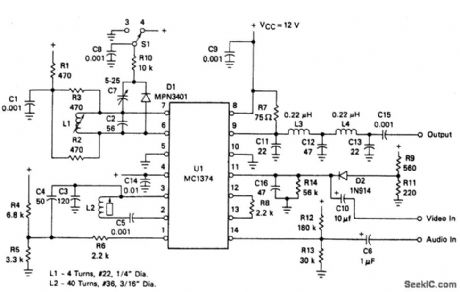
MICRO_TV_TRANSMITTER
Published:2009/6/24 21:19:00 Author:May
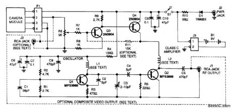
For very low power noncritical applications, this small TV modulator can be useful as a shortrange (50 feet) transmitter for video signals. A small camera module can be used as a source. R11 is used to vary dc offset of the modulator. (View)
View full Circuit Diagram | Comments | Reading(0)
TV_HORIZONTAL_DEFLECTION_CIRCUIT
Published:2009/6/23 2:34:00 Author:May
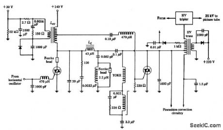
The circuit illustrates the method of using two SCR devices in a TV horizontal deflection application. This circuit was widely used by certain TV manufacturers as an alternate to the vacuum tube or transistor deflection circuit. (View)
View full Circuit Diagram | Comments | Reading(3542)
TELEVISION_VERTICAL_DEFLECTION_CIRCUIT
Published:2009/6/22 23:40:00 Author:May
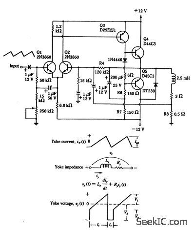
Two transistors are used to drive the yoke(2.5 mH + 0.3Ω) in this deflection circuit. R8 samples the yoke current and provides feedback to Q2, resulting in a very linear current ramp through the yoke. (View)
View full Circuit Diagram | Comments | Reading(0)
| Pages:1/2 12 |
Circuit Categories
power supply circuit
Amplifier Circuit
Basic Circuit
LED and Light Circuit
Sensor Circuit
Signal Processing
Electrical Equipment Circuit
Control Circuit
Remote Control Circuit
A/D-D/A Converter Circuit
Audio Circuit
Measuring and Test Circuit
Communication Circuit
Computer-Related Circuit
555 Circuit
Automotive Circuit
Repairing Circuit