
Signal Processing
Index 131
PINK_NOISE_GENERATOR
Published:2009/6/26 2:12:00 Author:May
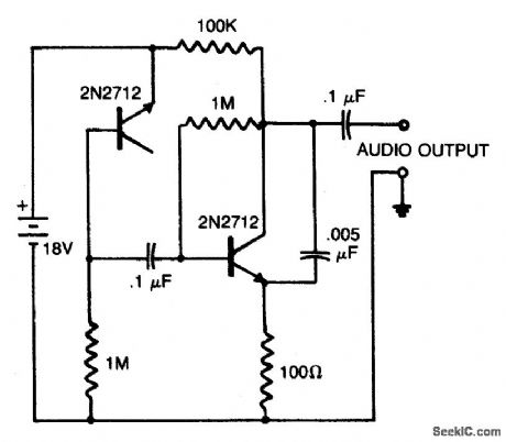
A reverse-biased pn junction of a 2N2712 transistor is used as a noise generator. The second 2N2712 is an audio amplifier. The 0.005 μF capacitor across the amplifier output remove s some high-frequency components to simulate pink noise more closely. The audio output may be connected to high-impedance earphones or to a driver amplifier for speaker listening. (View)
View full Circuit Diagram | Comments | Reading(0)
AUDIO_NOISE_GENERATOR
Published:2009/6/26 2:10:00 Author:May

This simple circuit generates both white and pin noise. Transistor Q1 is used as a zener diode. The normal base-emitter junction is reverse-biased and goes into zener breakdown at about 7 to 8 volts. The zener noise current from Q1 floirs into the base of Q2 such that an output of about 150 millivolts of white noise is available. To convert the white noise to pink, a filter is required which provides a 3 dB cut per octave as the frequency increases.Since such a filter attenuates the noise considerably an amplifier is used to restore the output level. Transistor Q3 is this amplifier and the pink noise filter is connected as a feedback network. between collector and base in order to obtain the required characteristic by controlling the gain-yersus-fre quency of the transistor. The output of transistor Q3 is thus the pink noise required and is fed to the relevant output socket. (View)
View full Circuit Diagram | Comments | Reading(3015)
ASTABLE_OSCILLATOR
Published:2009/6/26 1:59:00 Author:May
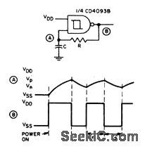
Before power is applied, the input and output are at ground potential and capacitor C is discharged. On power-on, the output goes high (VDD) and C charges through R until Vis reached. the output then goes low (VSS). C is now discharged through R until Vn is reached.The output then goes high and charges C towards Vp through R. Thus input A alternately swings between Vp and Vn as the output goes high and low. This circuit is self-starting at power-on. (View)
View full Circuit Diagram | Comments | Reading(913)
TONE_DIAL_GENERATOR
Published:2009/6/25 22:12:00 Author:May
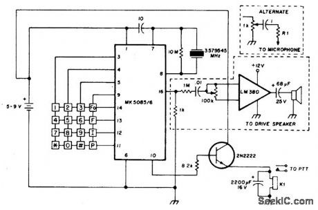
The circuit requires a minimum of parts and uses a low cost standard 3.579545-MHz television color-burst crystal. The speaker can be eliminated and the output fed directly into the microphone input of a transmitter. (View)
View full Circuit Diagram | Comments | Reading(945)
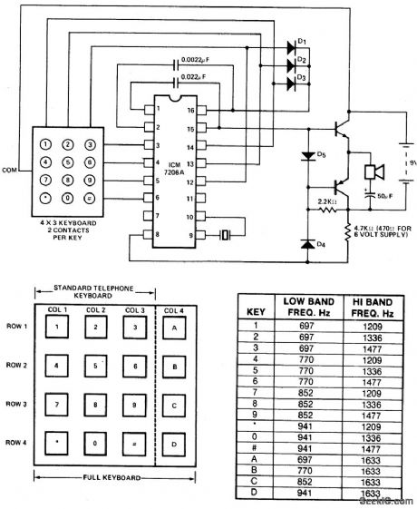
PORTABLE_TONE_GENERATOR
Published:2009/6/25 21:58:00 Author:May
View full Circuit Diagram | Comments | Reading(653)
CMOS_OSCILLATOR
Published:2009/6/25 21:34:00 Author:May
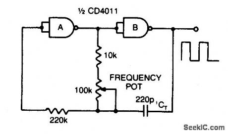
Varying the 100 K pot changes the discharge rate of CT and hence the frequency. A square wave output is generated. The maximum frequency using CMOS is limited to 2 MHz. (View)
View full Circuit Diagram | Comments | Reading(150)
SQUARE_WAVE_OSCILLATOR
Published:2009/6/25 21:24:00 Author:May
View full Circuit Diagram | Comments | Reading(0)
1_kHz_SQUARE_WAVE_OSCILLATOR
Published:2009/6/25 21:22:00 Author:May
View full Circuit Diagram | Comments | Reading(0)
R_C_OSCILLATOR
Published:2009/6/25 21:21:00 Author:May
View full Circuit Diagram | Comments | Reading(0)
SOUND_EFFECT_GENERATOR
Published:2009/6/25 21:10:00 Author:May
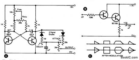
This waveshape generator is basically a slow running oscillator with variable attack and decay. A variable amplitude (high impedance) output is available via the 2 M potentiometer. B shows an add-on circuit which should be used if a low impedance output is required. Some of the output waveforms that can be produced are shown in C. (View)
View full Circuit Diagram | Comments | Reading(907)
MUSICAL_CHIME_GENERATOR
Published:2009/6/25 21:09:00 Author:May
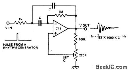
The circuit is that of a multiple feedback bandpass filter. A short click (pulse), makes it ring with a frequency which is its natural reso-nance frequency. Oscillations die away expo-nentially and closely resemble many naturally occuring percussive or plucked sounds. The higher the Q the longer the decay time constant. H igh frequencyre sonance s re semble chimes, lower frequencies sound like claves or bongos. Several circuits, all with different tuning, driven by pulses from a rhythm generator can produce an interesting pattern of sounds. (View)
View full Circuit Diagram | Comments | Reading(964)
TONE_BURST_GENERATOR
Published:2009/6/25 21:09:00 Author:May
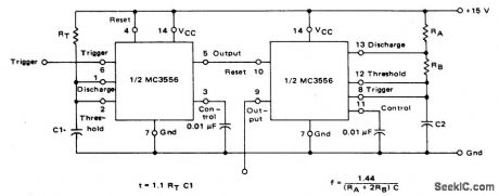
The first timer is used as a monostable and determines the tone duration when triggered by a positive pulse at pin 6. The second timer is enabled by the high output of the monostable. It is connected as an astable and determines the frequency of the tone. (View)
View full Circuit Diagram | Comments | Reading(0)
LASER_DIODE_PULSER
Published:2009/6/25 21:08:00 Author:May
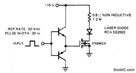
This drive is capable of driving the laser diode with 10 ampere, 20 ns pulses. For a 0.1% duty cycle, the repetition rate will be 50 kHz. A complementary emitter-follower is used as a driver. Switching speed is determined by the ft of the bipolar transistors used and the impedance of the drive source. (View)
View full Circuit Diagram | Comments | Reading(1569)
TIME_DELAY_GENERATOR
Published:2009/6/25 21:03:00 Author:May
View full Circuit Diagram | Comments | Reading(0)
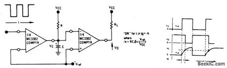
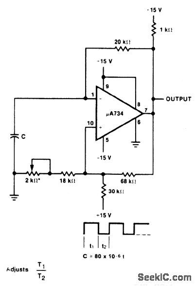
VERSATILE_TWO_PHASE_PULSE_GENERATOR
Published:2009/6/25 4:47:00 Author:May
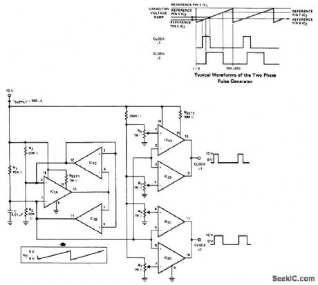
Two-phase clock generator uses two L161s to generate pulses of adjustable widths and phase relationships. Ramp generator feeds two variable window comparators formed by IC2A-IC2B and IC2C-IC2D respectively. (View)
View full Circuit Diagram | Comments | Reading(753)
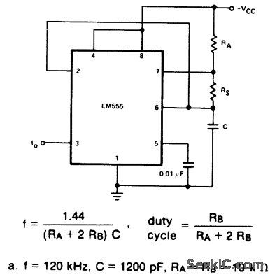
555_TIMER_OSCILLATOR
Published:2009/6/25 4:46:00 Author:May
View full Circuit Diagram | Comments | Reading(990)
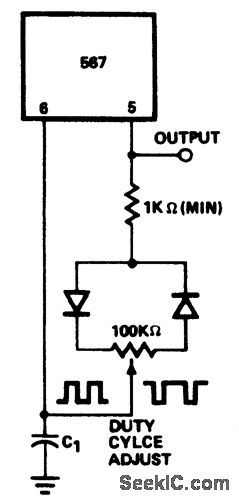
PULSE_GENERATOR_WITH_25%_DUTY_CYCLE_
Published:2009/6/25 4:45:00 Author:May
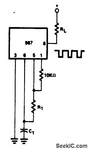
View full Circuit Diagram | Comments | Reading(852)
PULSE_GENERATOR_3
Published:2009/6/25 4:45:00 Author:May
View full Circuit Diagram | Comments | Reading(579)
FREE_RUNNING_OSCILLATOR_
Published:2009/6/25 4:44:00 Author:May
View full Circuit Diagram | Comments | Reading(782)
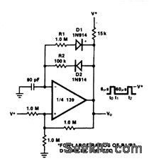
PULSE_GENERATOR_2
Published:2009/6/25 4:43:00 Author:May
View full Circuit Diagram | Comments | Reading(600)
| Pages:131/195 At 20121122123124125126127128129130131132133134135136137138139140Under 20 |
Circuit Categories
power supply circuit
Amplifier Circuit
Basic Circuit
LED and Light Circuit
Sensor Circuit
Signal Processing
Electrical Equipment Circuit
Control Circuit
Remote Control Circuit
A/D-D/A Converter Circuit
Audio Circuit
Measuring and Test Circuit
Communication Circuit
Computer-Related Circuit
555 Circuit
Automotive Circuit
Repairing Circuit