
Signal Processing
Index 125
PIERCE_CRYSTAL_OSCILLATOR
Published:2009/7/1 3:22:00 Author:May


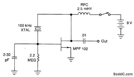
The JFET Pierce oscillator is stable and simple. It can be the clock of a microprocessor, a digital timepiece or a calculator. With a probe at the output, it can be used as a precise injection oscillator for troubleshooting. Attach a small length of wire at the output and this circuit becomes a micropower transmitter. (View)
View full Circuit Diagram | Comments | Reading(3212)
1_MHz_FET_CRYSTAL_OSCILLATOR
Published:2009/7/1 3:21:00 Author:May
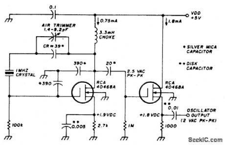
This stable oscillator circuit exhibits less than 1 Hz frequency change over a VDD range of 3-9 volts. Stability is attributed to the use of MOSFET devices and the use of stable capacitors. (View)
View full Circuit Diagram | Comments | Reading(2365)
CRYSTAL_OSCILLATOR
Published:2009/7/1 3:16:00 Author:May
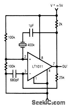
This circuit uses an LT1011 comparator biased in its linear mode and a crystal to establish its resonant frequency. This circuit can achieve a few hundred kHz, temperature independent clock frequency with nearly 50% duty cycle. (View)
View full Circuit Diagram | Comments | Reading(0)
FUNCTION_GENERATOR
Published:2009/7/1 3:16:00 Author:May
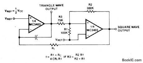
View full Circuit Diagram | Comments | Reading(0)
CRYSTAL_CONTROLLED_LOCAL_OSCILLATOR_FOR_SSB_TRANSMITTER
Published:2009/7/1 3:15:00 Author:May
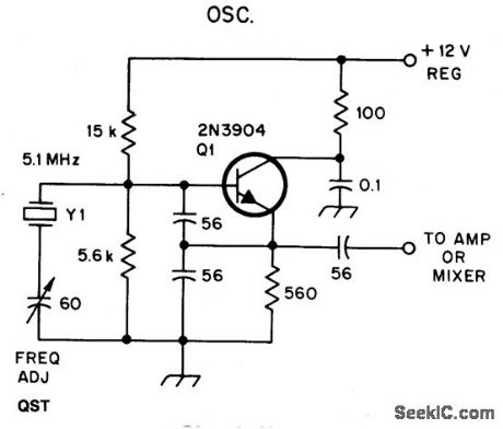


This oscillator may contain several switched crystals to provide channelized operation.A buffer amplifter may be added, if desired.
(View)
View full Circuit Diagram | Comments | Reading(924)
LOW_POWER,_5_V_DRIVEN,TEMPERATURE_COMPENSATED_CRYSTAL_OSCILLATOR(TXCO)
Published:2009/7/1 3:13:00 Author:May
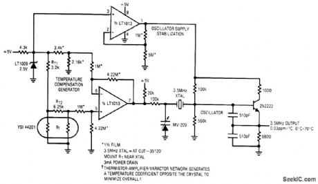
View full Circuit Diagram | Comments | Reading(843)
10_MHz_CRYSTAL_OSCILLATOR
Published:2009/7/1 3:11:00 Author:May


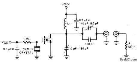
This xtal oscillator is a FET equivalent of a vacuum tube tuned to plate-tuned grid xtaloscillator. Feedback is via the drain to gate capacitance. (View)
View full Circuit Diagram | Comments | Reading(1070)
VARACTOR_TUNED_10_MHz_CERAMIC_RESONATOR_OSCILLATOR
Published:2009/7/1 3:09:00 Author:May
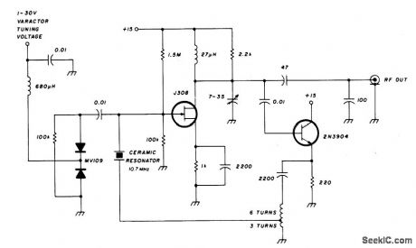
The FET input amplifier has fixed bias with source feedback. This provides a very high input impedance with very low capacitance. The FET amplifier drives an emitter follower which, in spite of the fact that it has a low output impedance, feeds a transformer with a 3:1 turns ratio for a nine-fold impedance reduction. The result is an impedance at the ceramic resonator of a few ohms maximum. The varactor-tuned ceramic resonator oscillator has a significant frequency-temperature coefficient. The tuning range of the VCO is approximately 232 kHz, with a temperature coefficient of 350 Hz per degree centigrade. When using this circuit as a VCO, the entire 232 kHz range cannot be used because some of the tuning range must be sacrificed for the temperature dependence.If the required tuning range were 200 kHz, leaving 32 kHz for temperature variation, the resulting temperature variation would be more than 90℃. (View)
View full Circuit Diagram | Comments | Reading(1950)
LINEAR_RAMP_GENERATOR
Published:2009/7/1 3:04:00 Author:May
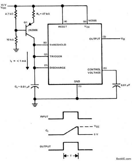
The linear charging ramp is most useful where linear control of voltage is required.Some possible applications are a long period voltage controlled timer, a voltage to pulse width converter, or a linear pulse width modulator. Q1 is the current source transistor, supplying constant current to the timing capacitor Ct. When the timer is triggered, the clamp on Ct is removed and Ct charges linearly toward VCC by virtue of the constant current supplied by Q1. The threshold at pin 6 is 2/3 VCC; here, it is termed VC. When the voltage across Ct reaches VC volts, the timing cycle ends. The timing expression for output pulse with T is:In general, It should be 1 mA value compatible with the NE555. (View)
View full Circuit Diagram | Comments | Reading(3256)
WAVEFORM_GENERATOR
Published:2009/7/1 2:55:00 Author:May
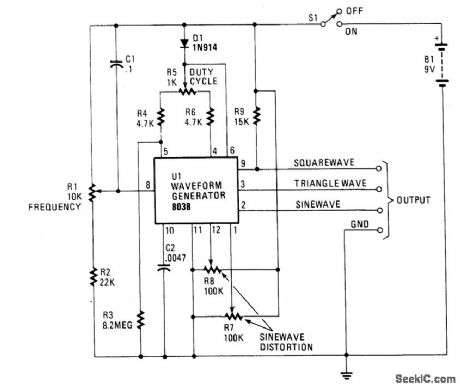
The circuit is designed around the Intersil 8038CC. Frequency range is approximately 20 Hz to 20 kHz-a tuning range of 1000:1 with a single control. The output frequency depends on the value of C2 and on the setting of potentiometer R1. Other values of C2 change the frequency range. Increase the value of C2 to lower the frequency. The lowest possible frequency is around.001 Hz and the highest is around 300 kHz. (View)
View full Circuit Diagram | Comments | Reading(1252)
Electrostatic_transducer_for_ultrasonic_measurement
Published:2009/7/24 4:11:00 Author:Jessie
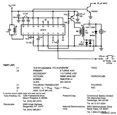
Pig. 14-23 The LM1812 is a complete ultrasonic transceiver used in a variety of pulse/echo-ranging applications. In this circuit, the LM1812 transmits a burst of oscillations with transducer X1. Then, using the same X1, listens for a return echo. If an echo of sufficient amplitude is received, the LM1812 detector produces a pulse (pin 16) of about the same width as the original burst. The closer the reflecting object, the earlier the return echo. Using the values and parts shown, the circuit has a range of about 4 inches to 30 feet. L6 resonates at 50 to 60 kHz, with the 500-pF capacitance of X1. L1 is tuned to this frequency by watching for maximum echo sensitivity with a scope at pin 1. National Semiconductor. Linear Applications Handbook 1991. p. 1173. (View)
View full Circuit Diagram | Comments | Reading(2741)
Fluid_level_control_system
Published:2009/7/24 4:10:00 Author:Jessie

Pig. 14-22 This circuit shows a simple system to control the emptying or filling process of a fluid container. The only transducers or probes involved are stainless-steel screws and hook-up wire (Fig. 14-22B). The fluid is drained by a motor-operated pump, which, in turn, is controlled by relay RY1. When the system is connected, as shown in Fig. 14-22A (for a sump or bilge pump), the pump motor (typically, a 1/4 HP) operates when the fluid level reaches the start probe, and continues until the level reaches the stop level. If the system is to control the filling process, use the circuit of Fig. 14-22C, National Semiconductor Linear Applications Handbook, 1991, p. 1169. (View)
View full Circuit Diagram | Comments | Reading(773)
High_performance_isolation_amplifier
Published:2009/7/24 4:09:00 Author:Jessie
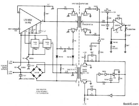
Fig. 14-21 This amplifier features inputs, which are galvanically isolated from the output and power connections, as required by many factory and process-control environments. The isolation allows this amplifier to ignore the effects of transducer ground loops, and operate at input common-mode voltages many times the power-supply voltage. The circuit has a 0.03% transfer accuracy, a 50-nV/℃ input drift, a gain of 1000, and will operate at 250-V input common-mode levels. To trim, tie the A1 input to floating common and adjust the zero trim for 0-V output. Next, connect the A1 input to +5-mV, and adjust the gain trim at A2 for +5.000-V output. Finally, connect the A1 input to -5 mV and select the 10-MΩvalue in the A2 feedback path for a -5.000-V output. Repeat as necessary. Linear Technology. Linear Applications Handbook, 1990.p. AN9-8. (View)
View full Circuit Diagram | Comments | Reading(921)
Level_detector_for_photodiode
Published:2009/7/24 4:16:00 Author:Jessie
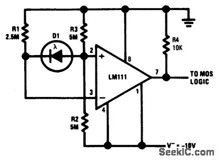
Fig. 15-3 This photodiode level detector operates from a single -10-V supply and is suitable for MOS logic. The output changes state when the D1 current reaches 1μA. Even at this low current, the error contributed by the LM111 is less than 1%. Higher threshold currents can be obtained by reducing R1, R2, and R3 proportionally. At the switching point, the voltage across D1 is nearly zero, so the D1leakage current does not cause an error. The output switches between ground and -10 V, The circuit will operate with a 5-V supply by reducing the values of R1, R2, and R3. Circuit accuracy depends on supply regulation because the reference is derived from the supply. National Semiconductor, Linear Applications Handbook 1991, p. 130. (View)
View full Circuit Diagram | Comments | Reading(890)
Zero_crossing_detector_for_magnetic_transducer
Published:2009/7/24 4:14:00 Author:Jessie
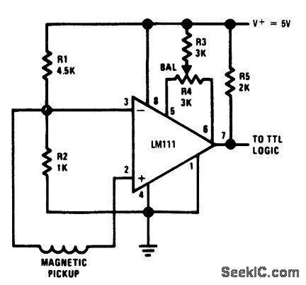
Fig, 15-2 This circuit detects zero crossing in the output of a magnetic transducer within a fraction of 1 mV. The resistive divider, R1 and R2, biases the inputs 0.5 V above ground, within the common-mode range of the LM111. The output will drive DTL or TTL directly. Because the output must drive any capacitive loading for positive-going output signals, the value of R5 determines circuit speed (a lower value increases speed). An optional offset-balancing circuit using R3 and R4 is included in the schematic. National Semiconductor Linear Applications Handbook 1991, p 130. (View)
View full Circuit Diagram | Comments | Reading(1926)
Basic_comparator
Published:2009/7/24 4:14:00 Author:Jessie
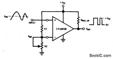
Fig. 15-1 This basic comparator circuit converts low-level analog signals to a high-level digital output. The pull-up resistor value should be high enough to avoid excessive power dissipation, yet low enough to supply sufficient drive to switch the load current at the comparator output. Resistors R1 and R2 set the input threshold trip voltage (VREF) at any value within the input common-mode range of the comparator. Notice that comparator common-mode characteristics are essentially the same as for op amps described in chapter 10. For example, with a VCC of 10 V, and both R1 and R2 at 5 kΩ, VREF can be set to any value up to 5V. National Semiconductor. Linear Applications Handbook, 1991, p. 257 (View)
View full Circuit Diagram | Comments | Reading(2129)
Comparator_for_ground_referred_load
Published:2009/7/24 4:22:00 Author:Jessie
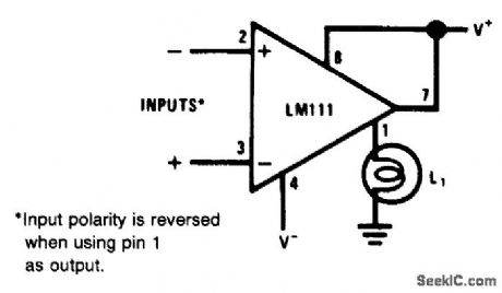
Fig. 15-8 This circuit uses a comparator to drive a ground-referred load, and it is useful during switching operations. An incandescent lamp draws a high inrush current when power is first applied (cold-filament resistance is typically 8 times slower than when the filament is heated). The high inrush current can damage a switch. The current limiting of the LM111 holds the inrush current to a safe level. Note that input polarity is reversed because the ground terminal of the LM111 is used as the output. National Semiconductor Linear Applications Handbook 1991, p. 1204. (View)
View full Circuit Diagram | Comments | Reading(691)
Zero_crossing_detector_for_MOS
Published:2009/7/24 4:21:00 Author:Jessie
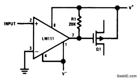
Fig. 15-7 In this zero-crossing detector, the ground terminal of the LM111 is connected to V-. With±15-V supplies, the signal swing delivered to the gate of Q1 is also ±15 V, so the circuit is well suited for MOS (particularly where the gain or feedback of a circuit must be changed at some precisely determined signal level). The circuit can be modified to work with JFETs. National semiconductor Linear Applications Handbook 1991, p 1204.
(View)
View full Circuit Diagram | Comments | Reading(825)
Interfacing_a_comparator_to_ECL
Published:2009/7/24 4:26:00 Author:Jessie
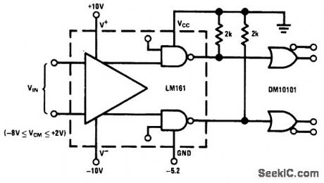
Fig. 15-12 This circuit shows how a high-speed comparator (LM161) that is designed for operation with TTL can be interfaced directly to ECL. National Semiconductor Linear Applications Handbook. 1991 p 326. (View)
View full Circuit Diagram | Comments | Reading(713)
Comparator_for_signals_of_opposite_polarity
Published:2009/7/24 4:25:00 Author:Jessie
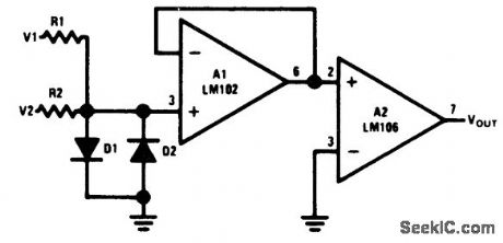
Fig. 15-11 In this circuit, R1 and R2 isolate the two signal sources. Often, such resistors must be relatively large so that the signal sources are not loaded (when fed directly to a comparator). As a result, the input current of the comparator must be reduced to prevent inaccuracies. The problem is eliminated with a buffer because the input current to the LM106 has no effect on the current through R1 and R2. National Semiconductor, Linear Applications Handbook. 1991, p. 1990. (View)
View full Circuit Diagram | Comments | Reading(651)
| Pages:125/195 At 20121122123124125126127128129130131132133134135136137138139140Under 20 |
Circuit Categories
power supply circuit
Amplifier Circuit
Basic Circuit
LED and Light Circuit
Sensor Circuit
Signal Processing
Electrical Equipment Circuit
Control Circuit
Remote Control Circuit
A/D-D/A Converter Circuit
Audio Circuit
Measuring and Test Circuit
Communication Circuit
Computer-Related Circuit
555 Circuit
Automotive Circuit
Repairing Circuit