
Signal Processing
Index 57
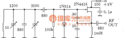
RC type scanning signal generator circuit composed of the FET tube
Published:2011/8/14 20:13:00 Author:TaoXi | Keyword: RC type, scanning signal, generator, FET tube
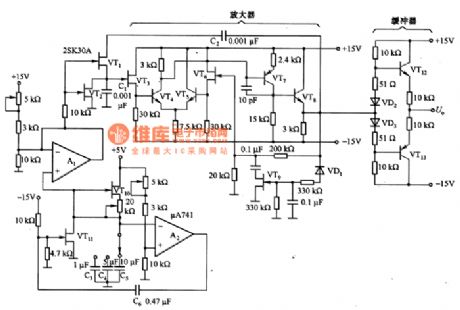
The RC type scanning signal generator circuit which is composed of the FET tube is as shown in the figure. This circuit is the Wien bridge RC oscillation circuit, and it is composed of the oscillation amplifier and the positive and negative feedback circuit. The oscillation frequency is decided by the RC value of the positive feedback circuit, now we suppose C=O.001μF to calculate the resistance of resistor R to see whether it meet the requirements.
The scanning circuit is composed of the constant current source, the constant current charging capacitor and the scanning discharging circuit, the VT10 constant current source charges the capacitors C3 - C5, when the charging voltage of the capacitor gets to a certain value, it will be compared by the comparator through the A2.
(View)
View full Circuit Diagram | Comments | Reading(1102)
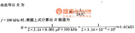
Audio frequency oscillator circuit diagram with adjustable frequency composed of μA741
Published:2011/8/10 4:26:00 Author:nelly | Keyword: Audio frequency oscillator, adjustable frequency
As shown in the figure, it is the audio frequency oscillator circuit with adjustable frequency. Beside using bulb control gain, the circuit also has the automatic gain control circuit which is composed of zener diodes D1, D2 and resistance R2. With the frequency's dropping, the output amplitude will increase. When the output amplitude increases to the preset value, then the zener diode turns on. So the amplifier's gain decreases, and it can avoid the amplifier saturating. R2 is used to decrease the amplitude limit of zener diode, then it can avoid excessive distortion.
(View)
View full Circuit Diagram | Comments | Reading(1437)
Sine wave signal source circuit diagram with stable output
Published:2011/8/10 6:50:00 Author:nelly | Keyword: Sine wave, signal source, stable output
As shown in the figure, it is the sine wave signal source with stable output. Firstly, using the primary operational amplifier comparator, and it produces a 60Hz constant amplitude square wave. The comparator's output terminal has a pair of 6.2V zener diodes which is connected back-to-back . The next is the two-stage Sallen-key type low pass filter, it can filter all the harmonic. The capacitance coupling amplifier separates the DC component which is produced by the unequal zener voltage in the limiter circuit, then it can compensate the filter's loss, and it accurately calibrates the output amplitude to 10V peak value.
(View)
View full Circuit Diagram | Comments | Reading(990)
SSB signal circuit diagram produced by phase-shift method
Published:2011/8/10 5:33:00 Author:nelly | Keyword: SSB signal, phase-shift method
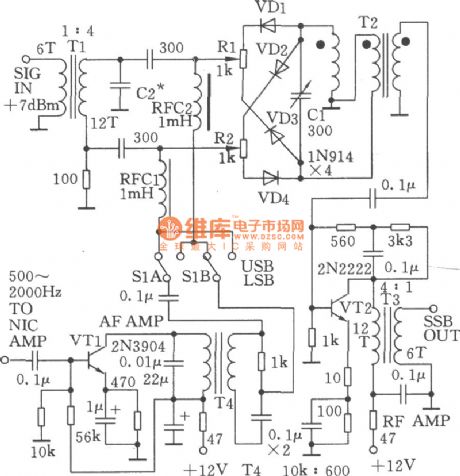
For HAM, it is a challenge to self-made SSB transmitter, it also is a test to self-power. At present, there is little HAM can self-made SSB transmitter at home, because the crystal filter and the crystal oscillator of SSB transmitter's core parts (such as the 8998, 5KHz, 9001, used in 9MHz crystal filter, 5KHz crystal oscillator)are hard to buy, in this case, it can adopt phase-shift method to produce SSB signal, compare to the common filter method, the phase-shift method is not so better to inhibit the uselessness side band.
(View)
View full Circuit Diagram | Comments | Reading(2678)
Low frequency Wien bridge sine wave oscillator(MC1456、μA741)circuit diagram
Published:2011/8/10 4:59:00 Author:nelly | Keyword: Wien bridge, sine wave, oscillator
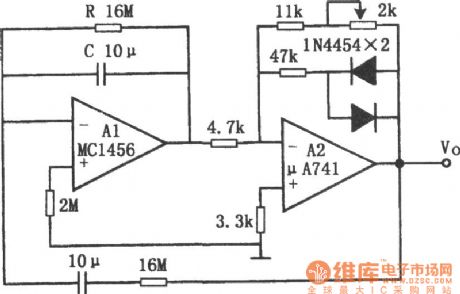
As shown in the figure, it is the low frequency Wien bridge sine wave oscillator circuit. This circuit adopts diode's index-number characteristic to stabilize the amplitude of 0.001Hz sine wave generator, then it has not large time constant, because the diode can quickly change their equivalent dynamic resistance. This stable circuit is similar to the limiter. The 47KΩ resistance which is in series with diode is used to decrease the diode's amplitude limit, and it can prevent circuit distortion. In general Wien bridge oscillator, due to the influence of operational amplifier's limited input impedance.
(View)
View full Circuit Diagram | Comments | Reading(3363)
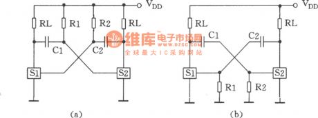
The reverse phase dual triangle wave generator
Published:2011/8/17 20:35:00 Author: | Keyword: Reverse phase, dual triangle wave, generator
View full Circuit Diagram | Comments | Reading(841)
The oblique wave generator formed by CD4046
Published:2011/8/17 20:33:00 Author: | Keyword: Oblique wave, generator
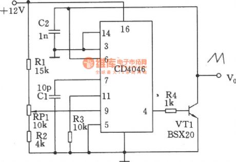
The oblique wave generator circuit is shown in the picture. It uses two capacitors to finish charging and discharging, which is C2 (connected to pin 6) and C1 (connected to pin 7). The ratio of capability of these two capacitors is 1000:1. When the charging time is shorter than discharging time, it generates a wave whose rising time is 1000 times of lowering time, which is actually the signal of saw wave. (View)
View full Circuit Diagram | Comments | Reading(1792)
Classic Cyle circuit
Published:2011/8/14 7:39:00 Author:leo | Keyword: Classic Cyle circuit
View full Circuit Diagram | Comments | Reading(793)
The multi-wave shape generator formed by CD4046
Published:2011/8/14 7:31:00 Author:leo | Keyword: Multi-wave shape, generator
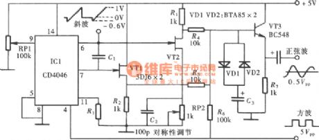
This wave generator can output square wave, sine wave and divergent wave.
(View)
View full Circuit Diagram | Comments | Reading(4617)
The impulse spreading circuit made by gatecircuits
Published:2011/8/17 20:37:00 Author: | Keyword: Impulse spreading circuit, gatecircuits
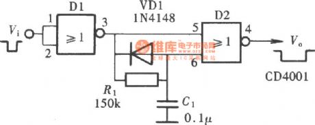
View full Circuit Diagram | Comments | Reading(784)
The triangular wave generator made by CD4046
Published:2011/8/17 20:41:00 Author: | Keyword: Triangular wave, generator
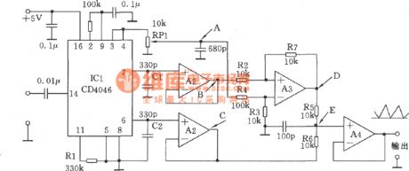
As the picture shows, this circuit can use to generate the triangular wave with fixed amplitude and based on earth potential. Its frequency can follow the frequency of PLL input signal. (View)
View full Circuit Diagram | Comments | Reading(2084)
The oscillator formed by CC4066
Published:2011/8/14 5:48:00 Author:leo | Keyword: Oscillator
As the picture shows, this is an oscillator made by CMOS analog electronic switch CC4066. The circuit in the picture is formed by two electronic switches. The frequency of this oscillator is decided by resistance components. When the R1 =R2 and C1=C2, the circuit generates square wave and f=1/2RC. (View)
View full Circuit Diagram | Comments | Reading(1945)
Square wave oscillator(741)
Published:2011/8/14 7:06:00 Author:leo | Keyword: Square wave, oscillator
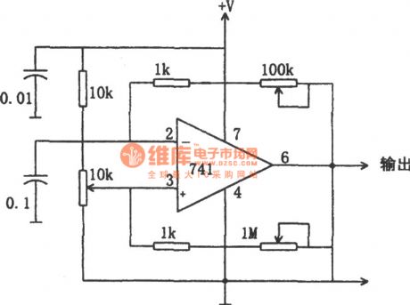
As the picture shows, this is an oscillator of square wave. It can generate the square wave with more than 100 to 1000 Hz frequency. Its frequency can be adjusted through resistor with 100kohms and 1Mohms. And the linearity of its output square wave is adjusted by resistor with 10kohms. If it only outputs at the same frequency, it can use fixed resistor to replace 100kohms and 1Mohms resistors. (View)
View full Circuit Diagram | Comments | Reading(2091)
The frequency divider circuit with a rate of 18 and made by CD4017
Published:2011/8/14 7:10:00 Author:leo | Keyword: Frequency divider, rate
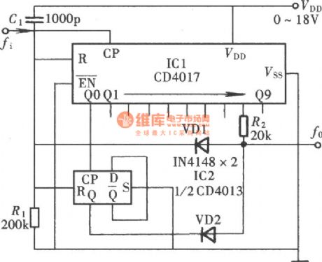
View full Circuit Diagram | Comments | Reading(2330)
The voltage follower circuit diagram
Published:2011/8/11 2:14:00 Author:Rebekka | Keyword: voltage follower
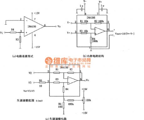
The figure shows the integration op-amp. When the input signal is too big, it may cause damage, even if integrated chip is not damaged, its work state have entered the nonlinear area. Figure (a) shows the circuit of the input signal to + l00V which is still working. The input voltage Vi increased to 3 pins. This circuit is the same phase, its input magnification is + 1, integrated chips is INA106, the chip is specially used for high voltage input follower. It normally uses withourt resistance. (View)
View full Circuit Diagram | Comments | Reading(925)
PSB8592 Microcomputer dial integrated circuit diagram
Published:2011/8/16 3:13:00 Author:Rebekka | Keyword: Microcomputer dial , integrated circuit
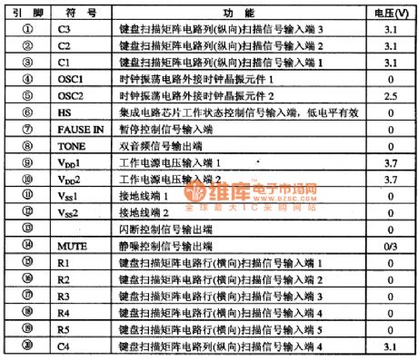
PSB8592 is microcomputer dial integrated circuit. It is applied to all communications for the use of dialing.
PSB8592 integrated circuit includes dial-up signal generation, coding and decoding key basins. It uses 20-pin dual in-line package, the pin functions and data of integrated circuit are listed in Table 1. (View)
View full Circuit Diagram | Comments | Reading(742)
The self-halt hypnomelder circuit
Published:2011/8/17 22:43:00 Author: | Keyword: self-halt hypnomelder
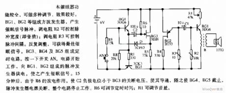
The hypnomelder is full-functioned, and it can do many adjustments, the effect is also good. The square wave generator consists of BG1 and BG2, which can generate the hypnosis signal pulse. By adjusting resistor R2, the pulse width (i.e tune quality) can be controlled; by adjusting resistor R3, the pulse interval can be controlled. The best hypnosis signal can be got by repeated adjustment. By press switch AN, the circuit begins to work, it powers the pulse generator composed of BG1 and BG2, which makes the generator generate hypnosis signals.
(View)
View full Circuit Diagram | Comments | Reading(822)
The multi-function electric stimulation therapeutic apparatus circuit
Published:2011/8/18 3:49:00 Author: | Keyword: multi-function, electric stimulation, therapeutic apparatus
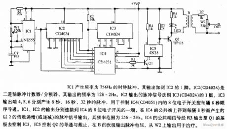
IC1 generates the clock pulse of 256Hz, and its output is added on the 1-pin of IC2. IC2(CD4024) is a binary pulse counter/frequency distributor, whose output frequency is 128~2Hz. The pulse signal output by IC2 is sent to the 1-pin of IC3(CD4024), the output terminals of 4, 5 and 6 generate the pulses of 8s, 16s and 32s respectively, which are to control the 8-bit electric switch in IC4(CD4051) and make the switch conducted every 8s in sequence. The output of IC1 and IC2 are linked to one terminal of IC4 8-bit e-switch. (View)
View full Circuit Diagram | Comments | Reading(2399)
The generating circuit based on sine waves
Published:2011/8/11 8:17:00 Author:Borg | Keyword: generating circuit, sine waves
The generating circuit based on sine waves is shown as above.
(View)
View full Circuit Diagram | Comments | Reading(940)
The sine wave oscillator circuit based on stability
Published:2011/8/11 8:19:00 Author:Borg | Keyword: sine wave oscillator, stability

The sine wave oscillator circuit based on stability is shown as above.
(View)
View full Circuit Diagram | Comments | Reading(811)
| Pages:57/195 At 204142434445464748495051525354555657585960Under 20 |
Circuit Categories
power supply circuit
Amplifier Circuit
Basic Circuit
LED and Light Circuit
Sensor Circuit
Signal Processing
Electrical Equipment Circuit
Control Circuit
Remote Control Circuit
A/D-D/A Converter Circuit
Audio Circuit
Measuring and Test Circuit
Communication Circuit
Computer-Related Circuit
555 Circuit
Automotive Circuit
Repairing Circuit