
Basic Circuit
Index 140
INCANDESCENT_LAMP_LIFE_EXTENDER
Published:2009/7/14 12:26:00 Author:May
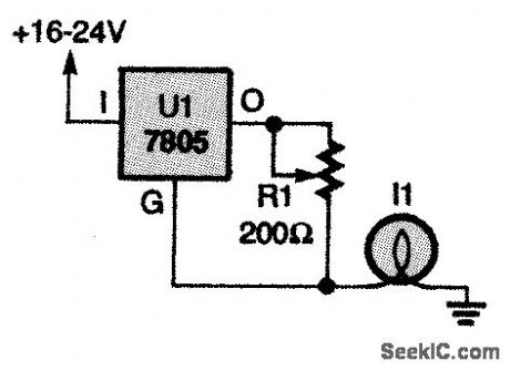
The cold resistance of an incandescent lamp is normally very low compared to its operating resistance. Each time such a lamp is turned on, the initial current is several times greater than its rated operating current. The life-extender circuit will work with any incandescent lamp that operates at a voltage of 1.5 to 12 V and a current of 1 A or less. Look up the lamp's normal operating current and, using an ammeter, set R1 so that the normal operating current flows to the lamp. Now, each time the lamp is switched on, the initial current will be limited to its preset value. (View)
View full Circuit Diagram | Comments | Reading(1063)
CHRISTMAS_LIGHT_DIMMER
Published:2009/7/14 12:25:00 Author:May
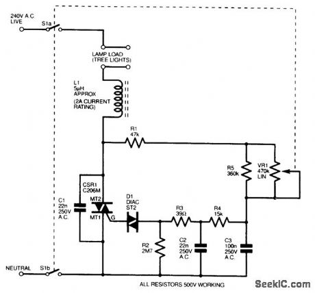
This is based on a standard diac/triac dimmer configuration, which has been optimized for this application. Resistor R2 is, however, optional and was included only to help discharge the capacitors quickly. All capacitors are 260-Vac X2 rated (this is very importctnt), all resistors are 500-V working voltage, and triac CSR1 was chosen for its low holding current so that it would function with small loads. Note that VR1 is fitted with a double-pole mains switch for complete isolation. Even with only one 20-lamp string plugged in (22 W), control is very smooth with barely any trace of hysteresis. This circuit can be built safely on a piece of matrix board, wired point-to-point, provided it is mounted in a completely insulated plastic case and that no external components (i.e.,S1 and VR1) are metal.(Do not build this circuit if you do not understand the safety requirements.) (View)
View full Circuit Diagram | Comments | Reading(1162)
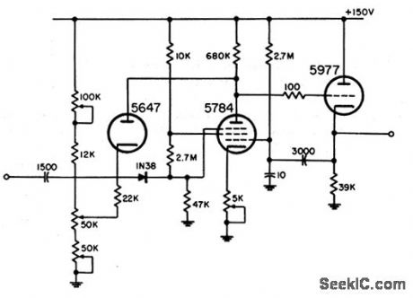
R_Y_TEST_GENERATOR
Published:2009/7/15 0:41:00 Author:Jessie
Uses ICs rather than PROM for automatic generation of sequence of 64 alternating Rs and Ys, plus Baudot codes for carriage return and line feed, as used for testing radioteletype equipment. Circuit in dashed lines generates codes for printing R and Y continuously without regard for line length. Jumper J1 gives choice of normal or inverted output data for keying transmitter with either mark-high or space-high signal. Operates at slightly less than 60 WPM Adjust R1 so clock pulse generator U1 runs at 45.45 Hz Article covers construction and operation-J,Loughmiller ,RTTY Test Generator,Ham Radio.Jan 1978,p 64-66. (View)
View full Circuit Diagram | Comments | Reading(752)
DC_LAMP_DIMMER
Published:2009/7/14 12:16:00 Author:May
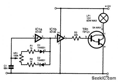
The dc lamp dimmer circuit will adjust the brightness of a dc lamp or the speed of a suitable dc motor. An oscillator is formed around Schmitt inverter IC1a, and is buffered by IC1b. This, in turn, drives TR1, which is a Darlington power transistor. The lamp LP1 forms the collector (c) load for the transistor, and this is driven at a nominal 330 Hz. The duty cycle is, however, fully variable using potentiometer VR1. Consequently, the power delivered to the load can be controlled between 5 and 95 percent, approximately. No flicker will be apparent at this frequency. The circuit consumes little power itself and is ideal for controlling car instrument panel lights. (View)
View full Circuit Diagram | Comments | Reading(3189)
300_AND_1800_BAUD_FSK_DEMODULATOR
Published:2009/7/15 0:30:00 Author:Jessie
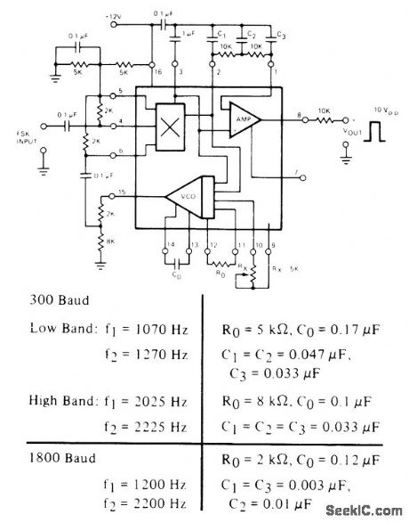
Uses Exar XR-215 PLL IC having frequency range of 0.5 Hz to 35 MHz. When input frequency is shifted by data bit, DC voltage between pins 2 and 3 reverses polarity. Opamp section is connected as comparator for converting DC level shift to binary output pulse. C1 serves as PLL filter. C2 and C3 are postdetection filters. Table gives typical values of components for two transmission speeds.- Phase-Locked Loop Data Book, Exar Integrated Systems, Sunnyvale, CA. 1978. p 21-28. (View)
View full Circuit Diagram | Comments | Reading(852)
NONPRECISE_PHANTASTRON_VARIABLE_DELAY_2
Published:2009/7/15 2:04:00 Author:Jessie
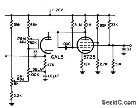
Used to delay beginning of crt sweep for expanded display range is 5 to 175 miles. Trailing edge of screen waveform is differentiated and used to trigger blocking oscillator through trigger amplifier.-NBS, Handbook Preferred Circuits Navy Aeronautical Electronic Equipment, Vol.1.Electron Tube Circuits,1963,p N9-3 (View)
View full Circuit Diagram | Comments | Reading(595)
SELF_GENERATING_FSK
Published:2009/7/15 2:03:00 Author:Jessie
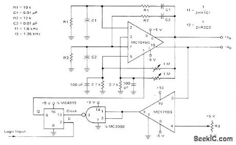
Dual oscillators in Motorola MC1545G gated video amplifier are used with external frequency-determining components R1C1 and R2C2 to give 1.6 kHz for fl and 1.35 kHz for f1. Logic switching network compares output to reference and updates gate input with each cycle of output. Circuit gives smaller switching transients than are possible with separate oscillators because one oscillator is driven at frequency of the other while first oscillator is of. R3 sets transition to any level desired.- Gated Video Amplifier Applications-the MC1545, Motorola, Phoenix, AZ, 1976, AN-491, p 13. (View)
View full Circuit Diagram | Comments | Reading(814)
PULSE_WIDTH_M_O_D_U_L_A_T_O_R
Published:2009/7/15 2:03:00 Author:Jessie
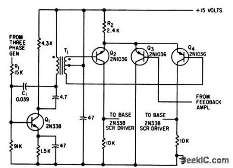
Determines length of quasi-square waves used in con nection with triggering of scr's in output stage of inverter.-R. J. Kearns and J. J. Rolfe, Three-Phase Static Inverters Power Space-Vehicle Equipment, Electronics, 34:18, p 70-73. (View)
View full Circuit Diagram | Comments | Reading(960)
NONPRECISE_PHANTASTRON_VARIABLE_DELAY_1
Published:2009/7/15 2:02:00 Author:Jessie
Used to delay beginning of crt sweep for expanded display. Range is 5 to 175 miles. Trailing edge of screen waveform is differentiated and used to trigger blocking oscillator through trigger amplifier.-NBS, Handbook Preferred Circuits Navy Aeronautical Electronic Equipment, Vol. 1, Electron Tube Circuits, 1963, p N9-3. (View)
View full Circuit Diagram | Comments | Reading(663)
170_OR_850_Hz_SHlFT
Published:2009/7/15 2:01:00 Author:Jessie
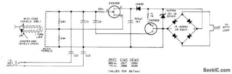
Simple AF RTTY keyer uses 2N5823 silicon PNP transistor switch instead of optical coupler. Short piece of coax serves as 1-turn output link. Outer shield is grounded only at coaxial connector so braid acts as Faraday shield, eliminating capacitive signal and noise pickup from circuit.-E. Noll, Circuits and Techniques, Ham Radio, April 1976, p 40-43.
(View)
View full Circuit Diagram | Comments | Reading(1114)
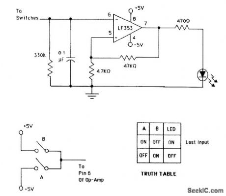
DIGITAL_LATCH_WITH_SAFETY_RESET_FEATURE
Published:2009/7/14 12:08:00 Author:May
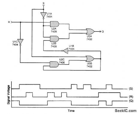
The time diagram illustrates the various modes of operation of the circuit. A high S input causes the output (Q) to go low. Thereafter, a high R input can reset Q to high, but only so long as S remains low.The asynchronous digital latching circuit is designed for use in a safety-related application, like turning off power in response to an alarm signal. During normal operation in the absence of an alarm, the SET (S) and RESET input voltages are low or off, while the output voltage (Q) is high or on. The SET input constitutes the alarm signal: Whenever S goes high (on), Q goes low (off), and thereafter remains low, even when S goes low. Thus, for example, the circuit keeps a power supply turned off even when the alarm has been shut off. If a safe condition has been restored, then the circuit can be reset to Q high by applying a high (on) signal to the RESET ( R ) input terminal. However, regardless of the R input level, Q cannot be driven high as long as S remains high; that is, the circuit cannot be reset if the alarm signal is still on. Thus, the RESET signal cannot override the alarm signal and thereby provide a false indication of safety. Also, this does not go into oscillation when the SET and RESET inputs change simultaneously.
(View)
View full Circuit Diagram | Comments | Reading(1103)
DC_D_C
Published:2009/7/15 2:01:00 Author:Jessie
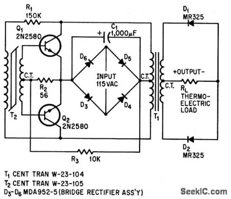
Line voltage is rectified, inverted at 18 kc, stepped down, and rectified to give 23 a at 6 v for thermoelectric heat-pump system.-A. L. Wennerberg and F. H. Schroedet, High-Current Converter is Small, Quiet, Low-Cost, Electronics, 37:30, p 41. (View)
View full Circuit Diagram | Comments | Reading(782)
PB_SWITCH_ACTIVATED_LATCH
Published:2009/7/14 12:04:00 Author:May
View full Circuit Diagram | Comments | Reading(602)
SELF_EXCITED_3_PHASE_NON_PHASE_AMBIG_UOUS_BRIDGE
Published:2009/7/15 2:06:00 Author:Jessie
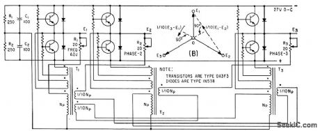
Each oscillating section is half-bridge converter operating in square-wave mode. Phase diagram shows derivation of synchronizing voltages.-A. G. Lloyd, Half-Bridge Inverter Provides Economical Three-Phase Power, Electronics, 34:37, p 62-65. (View)
View full Circuit Diagram | Comments | Reading(649)
O_TO_2440_MICROSEC_PHANTASTRON_DELAY
Published:2009/7/15 2:06:00 Author:Jessie
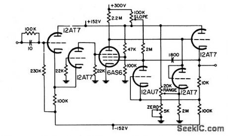
Is triggered by gating mvbr. Receives control voltage from ten-turn potentiometer calibrated in distance units. Output drives blocking oscillator through transformer. Accuracy is about 1% of delay setting.-NBS, Hand-book Preferred Circuits Navy Aeronautical Electronic Equipment, Vol. 1, Electron Tuba Circuits, 1963, p N9-2. (View)
View full Circuit Diagram | Comments | Reading(628)
LASER_MODULATION
Published:2009/7/14 11:51:00 Author:May
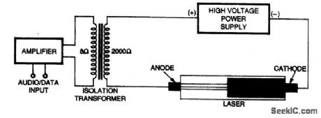
Electronic modulation of a laser beam can be handled in this fashion. Obviously, the transformer you use must be able to handle the high voltage from the laser power supply without breaking down. (View)
View full Circuit Diagram | Comments | Reading(1107)
SINGLE_HETEROSTRUCTURE_LASER_DRIVER
Published:2009/7/14 11:44:00 Author:May
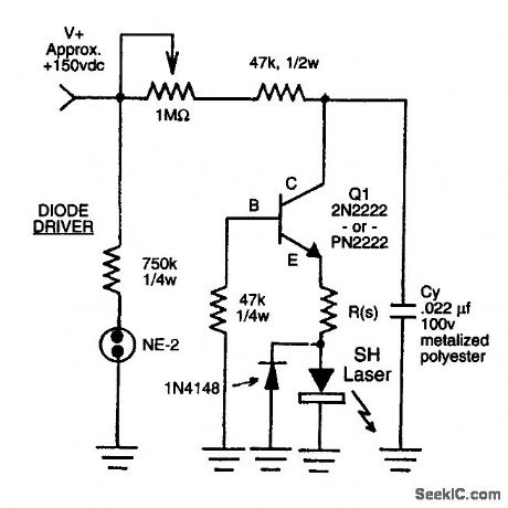
One way to reliably achieve the fast rise-time pulse of short duration to power SH lasers is to use the phenomenon called avalanching of a transistor. Transistors have a breakdown voltage, abbreviated as Vceo; if this voltage is exceeded, the transistor will spontaneously conduct with its collectorto-emitter circuit open and the voltage applied to its collector. This produces a pulse whose rise time is extremely fast-on the order of 1 or 2 ns-and whose duration is related to the capacitance at the collector. The operation is as follows: Current rises at the base of transistor Q1 when the voltage on Cy has risen enough to jump over and break down the collector-to-emitter junction. For the 2N2222, this is typically 75 to 80 V. When the transistor breaks down, it sends a high-current pulse of energy through a low-value carbon film resistor R(s). With the 0.022-μF capacitor shown, the duration of the pulse to the laser is only about 75 ns. This capacitor must be specifically designed for low inductance. Note the high-speed switching diode D1. Its purpose is to damp out any reverse voltage that might occur in the circuit due to inductance after the laser turns off because a reverse voltage of only 3 V can destroy the SH laser. The rise time of this diode is comparable to that of the avalanche circuit, being only 6 ns before it begins to switch. The values of the capacitor and the current-limiting resistor R(s) depend upon the type of SH laser diode used. (View)
View full Circuit Diagram | Comments | Reading(1051)
LOW_COST_LASER_DIODE_DRIVER
Published:2009/7/14 11:41:00 Author:May
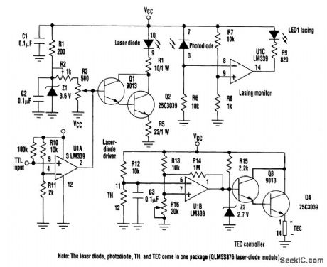
The circuit presented is a low-cost laser-diode driver with current limiting and a lasing monitor for safe operation of the laser. The driver provides temperature stabilization using a built-in thermoelectric-cooler (TEC) controller. This circuit is designed around a QLM5S876 1.55-m laser-diode module with a built-in monitor photodiode, TEC, and thermistor. The laser is driven by the constant-current source Q2 and Q1. The drive current is stabilized against supply changes by Z1, limited by R2, and adjusted by R3 to the desired operating point. When the current is small, the laser doesn't lase and the monitor photodiode detects no optical power. As a result, comparator U1C goes below its trip point and LED1 turns off. When the current is adjusted and passes the laser threshold, sufficient optical power is generated by the laser, causing photo current to flow through the photodiode and the comparator to drive the lasing monitor indicator LED1 to on. The TEC controller circuit is a feedback system. If the temperature is higher than the set point, the comparator output will be high and will drive the TEC element through R15, Q3, and Q4. The TEC drive current is limited by Z2. When the TEC is driven on, it cools the laser. This increases the voltage of the inverting output until it passes the comparator's upper trip point and turns off the TEC's drive current. The temperature set point can be adjusted by R16. (View)
View full Circuit Diagram | Comments | Reading(7084)
CASSETTE_RECORD_PLAYBACK
Published:2009/7/14 7:42:00 Author:May
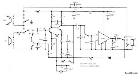
National LM389 power amplifier chip includes three NPN transistors, to provide all circuits needed for complete recording and playback of cassette tapes. Two of internal transistors act as signal amplifiers while third is used for automatic level contra when recording. Diode is also on chip.- Audio Handbook, National Semiconductor, Santa Clara, CA, 1977, p 4-33-4-37. (View)
View full Circuit Diagram | Comments | Reading(1261)
DELAYED_DROPOUT_RELAY_TIMER
Published:2009/7/15 3:25:00 Author:Jessie
Keeps relay energized for preset time of up to 10 sec after relay is pulled in by momentarily closing switch.- Transistor Manual, Seventh Edition, General Electric Co. 1964, p 324. (View)
View full Circuit Diagram | Comments | Reading(864)
| Pages:140/471 At 20121122123124125126127128129130131132133134135136137138139140Under 20 |
Circuit Categories
power supply circuit
Amplifier Circuit
Basic Circuit
LED and Light Circuit
Sensor Circuit
Signal Processing
Electrical Equipment Circuit
Control Circuit
Remote Control Circuit
A/D-D/A Converter Circuit
Audio Circuit
Measuring and Test Circuit
Communication Circuit
Computer-Related Circuit
555 Circuit
Automotive Circuit
Repairing Circuit