
TV Circuit
Index 2
ATV_VIDEO_SAMPLER_CIRCUIT
Published:2009/6/19 4:39:00 Author:May
This unit picks up your ATV signal by sampling the transmission line with negligible insertion loss. It uses 2 N connectors for input and output connections. A BNC connector is used on the video output. The detected output is connected to your rrtonitor and scope so that you can accu-rately adjust your transmitter for proper video and synch levels. TWo different models are provided.Both have relative power output meters, but one has greater accuracy. There are two PC controls, one for video level and the other for power output. (View)
View full Circuit Diagram | Comments | Reading(919)
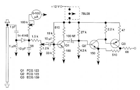
IR_ILLUMINATOR_FOR_NIGHT_VISION_TV_CAMERAS_AND_SCOPES
Published:2009/6/19 4:10:00 Author:May
This Source uses LEDs and an astable oscillat to control the switch,duty-cycle,and effective IR illumination output. (View)
View full Circuit Diagram | Comments | Reading(1948)
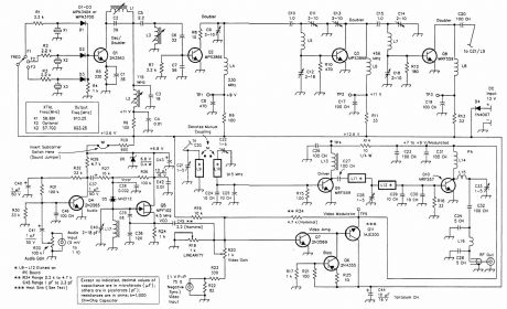
STEREO_TV_DECODER
Published:2009/6/18 23:51:00 Author:May

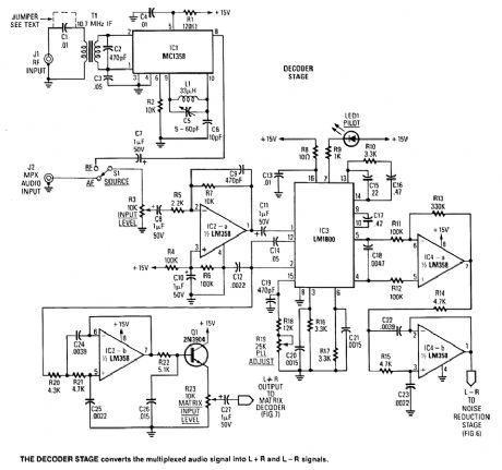
A block diagram of the stereo-TV decoder is shown in A. It shows the overall relationships be-tween the separate sections of the circuit; B through E show the details of each subsection. The de-coder section centers around IC1, a standard 4.5-MHz audio demodulator. The output of IC1 is routed to 51, which allows you to choose between the internally demodulated signal and an exter-nally demodulated one. Buffer amplifier IC2-a then provides a low-impedance source to drive IC3, an LM1800 stereo demodulator.When IC3 is locked on a stereo signal, the outputs presented at pins 4 and 5 are discrete left- and right-channel signals, respectively. In order to provide noise reduction to the L-R signal, you must recombine the discrete outputs into sum and difference signals. Op amp IC4-a is used to regenerate the L-R signal. It is wired as a difference amplifier, wherein the inputs are summed together (+L -,R). Capacitor C18 bridges the left- and right-channel outputs of the demodulator. Although it decreases high-frequency separation slightly, it also reduces high-frequency distortion.The L + R signal is taken from the LM1800 at pin 2, where it appears at the output of an internal buffer amplifier. The rawL -R signal is applied to IC4-b, a 12-kHz lowpass filter. The L + R signal is also fed through a 12-kHz low pass filter in order to keep the phase shift undergone by both signals equal.Next, the L - R signal is fed to Q2. It allows you to add a level control to the L - R signal path; it provides a low source impedance for driving the following circuits, and it inverts the signal 180°. In-version is necessary to compensate for the 180°inversion in the compander.Next comes the expander stage. At the collector of Q2 is a 75-μs de-emphasis network (R27 and C29) that functions just like the network that is associated with Q1. Note that Q2 feeds both Q3 and IC5-a, a -12-dB per octave high-pass filter. The output of that filter drives the rectifier input of IC6, an NE570. The 75-Hz high-pass filter at the rectifier input helps to prevent hum, 60-Hz sych buzz, and other low-frequency noise in the L - R signal from causing pumping or breathing.The NE570 contains an on-board op amp; its irtverting input is available directly at pin 5 and via a 20-kO series resistor at pin 6. The 18-kQ resistor (R30) combines with the internal resistor and C32 (0.01 μF) to form a first-order filter with a 390-μs time constant. Because the internal op amp oper-ates in the inverting mode, the -(L - R) signal is restored to the proper (L - R) form.The output of the expander drives another 75-Hz high-pass filter, but this one is a third-order type that provides -18 dB per octave rolloff. It is used to keep low-frequency noise from showing up at the output of the decoder. At this point, the (L - R) signal has been restored, more or less, to the condition it was in before it was dBx companded at the transmitter. (View)
View full Circuit Diagram | Comments | Reading(291)
ATV_DOWNCONVERTER_FOR_420_TO_450_MHz
Published:2009/6/18 5:02:00 Author:May
This ATV downconverter converts the 420- to 450-MHz ATV band, which is several channels be-tow the lower limit of the UHF band, to channel 3 or 4 for viewing on virtually any TV. The down-converter has a low-noise preamplifier stage and a double-balanced passive mixer for good performance and a wide dynamic range. That is necessary with today's crowded UHF bands. The converter draws about 27 milliamperes from a 13.2-volt dc source, so it can be used in portable and mobile applications. An extra IF stage gives an overall gain of about 25 dB. A block diagram of the clownconverter is also shown. A complete kit of parts, including PC board, is available from North Country Radio, P.O. Box 53, Wykagyl Station, New Rochelle, NY 10804-0053A. (View)
View full Circuit Diagram | Comments | Reading(1997)
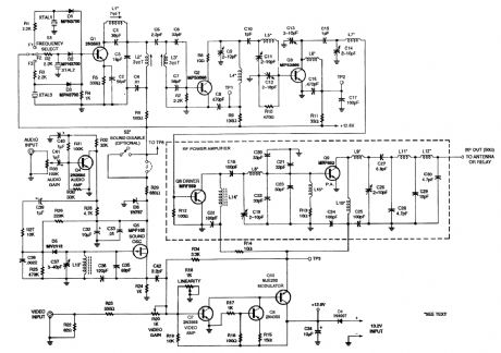
THREE_CHANNEL_420_TO_450_MHz_ATV_TRANSMITTER
Published:2009/6/18 4:59:00 Author:May
This transmitter is a 2-watt PEP output device for 420- to 450-MHz amateur TV operation. It has three crystal-controlled channels and will accept standard NTSC video input. It also has a 4.5-MHz sound subcarrier capability. Because this transmitter has AM modulation, audio can be transmitted in AM form on the RE carrier by applying audio to the video input. Bandwidth of audio can be restricted to 20 kHz by placing a 0.002-pF capacitor across R34. A complete kit of parts, including PC board is available from North Country Radio, P.O. Box 53, Wykagyl Station, New Rochelle, NY 10804-0053A. (View)
View full Circuit Diagram | Comments | Reading(2022)
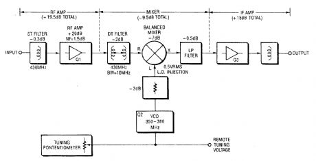
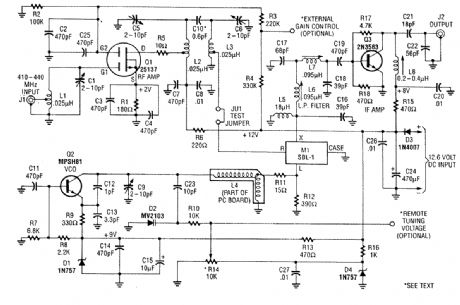
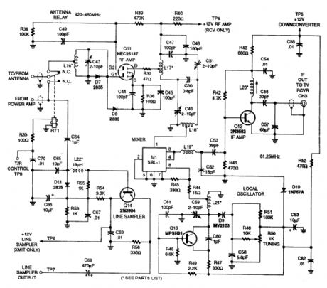
ATV_DOWNCONVERTER_FOR_902_TO_928_MHz
Published:2009/6/18 4:51:00 Author:May
This clownconverter converts ATV signals in the 902- to 928-MHz range to a 61.26- or 67.25-MHz IF output frequency (CH 3 or CH 4) to enable reception of these signals on a standard VHF TV receiver or monitor. It features a low-noise RF amp feeding a Schottky diode double-balanced mixer, a tunable LO and one IF preamp stage. The RF amplifier is a low-noise dual-gate GASFET that is followed by a sec-ond RE stage using an MMIC. Five tuned circuits are used in the RE amplifier. This feeds a packaged Schottlqr diode mixer assembly for better dynamic range and reduced susceptibility to intermodulation and strong signal areas. The on-board local oscillator (LO) is voltage tuned and if desired can be set up for remote tuning. Ail necessary circuitry for remote tuning is on board for coax dc and IF feed. This enables the clownconverter to be mast mounted to get around feedline losses generally associated with this frequency range. No separate dc feed is necessary because the coax (RG59/U recommended) carries dc power, tuning voltage, and IF signal. A dc block is used at the receiver for the purpose of separating dc voltage supply and the tuningvoltage. This allows a cable run of several hundred feet, if needed.By using this clownconverter and transmitter, a physically small915-MHz ATV station or even a video HT can be constructed because both units are each 2.50 x 4.00 inches x 1.00 high, and can be stacked together. A complete kit of parts, including PC board is available from North Country Radio, P.O. Box 53, Wykagyl Station, New Rochelle, NY 10804-0053A. (View)
View full Circuit Diagram | Comments | Reading(1466)
THREE_CHANNEL_902_TO_928_MHz_ATV_TRANSMITTER
Published:2009/6/18 4:42:00 Author:May
This transmitter is for ATV applications in the 902- to 928-MHz band. It has three crystal-con-trolled channels, and will accept standard NTSC video input. It also has a 4.5-MHz sound subcarrier.Because this is an lNI transmitter, audio can be transmitted as AM on the RF carrier. Simply use the video input Bandwidth。f audio can be restricted to dU kHz by placing a capacitor with a value of about o.002 pF across R34 The output is 1 5 to 2 watts PEP into a 50-Ω load,A complete kit of partsincluding PC board,is available from North Country Radio,P.O 0.Box 53,Wyktation,New Rochelle,NY 10804-0053A (View)
View full Circuit Diagram | Comments | Reading(1819)
MAST_MOUNTED_ATV_PREAMP
Published:2009/6/18 4:29:00 Author:May
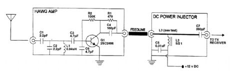
This simple ATV preamp covers the 427-to 439-MHz ATV frequencies and can be mast mounted and dc powered through the feedline. (View)
View full Circuit Diagram | Comments | Reading(1005)
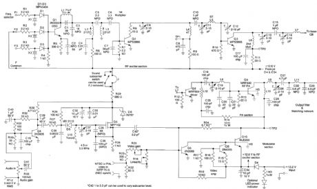
MINI_ATV_TRANSMITTER
Published:2009/6/18 3:52:00 Author:May
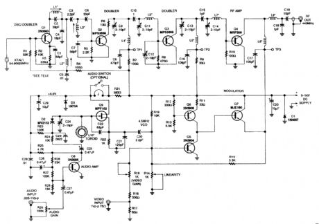
This low-power NTSC video and sound transmitter is useful for amateur radio, video handle-talkie, R/C and surveillance pur-poses. A crystal oscillator-multip lier RI' power amplifier. Video modulation is via a three-transistor series modulator. The sound subcarrier is generated with a VC0 circuit and is combined with the video information. The output is 0.4 to 1.2 W with supply volt-ages of 9 to 14 volts. A complete kit of parts, including PC board, is available from North Country Radio, P.O. Box 53, Wykagyl Sta-tion, New Rochelle, NY 10804-0053A. (View)
View full Circuit Diagram | Comments | Reading(2866)
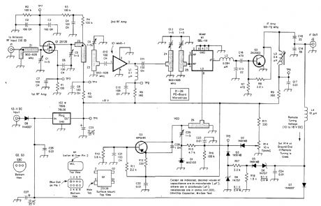
5_W_ATV_TRANSCEIVER
Published:2009/6/18 3:48:00 Author:May
For the transmitter schematic (part of this transceiver), see entry entitled S-W ATV Transmit-ter for 440 MHz, Fig. 5-1. The downconverter portion is shown here.This transmitter contains both a video and sound section. Five to six watts PEP on synch tips of NTSC video are produced. Three channels are available. Channel switching is via PIN diodes. Power supply voltage is 12 to 14 Vdc. The receiver function is provided with a downconverter circuit and is tunable. A relay is used for T-R switching. A complete kit of parts, including PC board, is available from North Country Radio, P.O.Box 53, Wykagyl Station, New Rochelle, NY 10804-0053A. (View)
View full Circuit Diagram | Comments | Reading(2122)
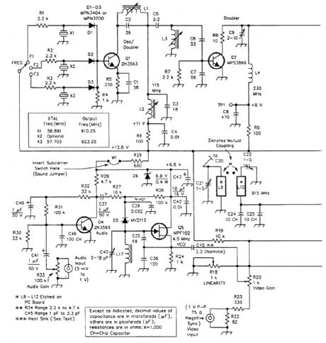
5_W_ATV_TRANSMITTER_FOR_440_MHz
Published:2009/6/18 3:45:00 Author:May
The circuit will produce typically 6 W RE output on synch tips. A crystal oscillator drives a doubler to produce a 220-MHz output.Another doubler produces 440 MHz to drive the power amplifier. A high-level series modulator provides the video modulation capa-bility. A sound subcarrier is generated using a VCO circuit and combined with the video information. A complete kit of parts, includ-ing the PC board, is available from North Country Radio, P.O.Box 53, Wykagyl Station, New Rochelle, NY 10804-0053A. (View)
View full Circuit Diagram | Comments | Reading(1752)
TV_SOUND_SYSTEM
Published:2009/6/18 1:43:00 Author:May
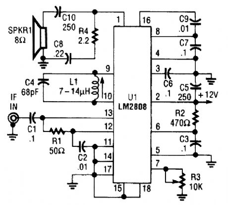
An LM2808 performs IF amplification of the 4.5-MHz sound subcarrier, limiting, detection, and audio amplification. If the center frequency must be changed, then change L1/C4. Audio out-put is 0.5 W. R3 is the volume control. (View)
View full Circuit Diagram | Comments | Reading(745)
TMPA8809 Multi-Function Super-Monolithic Integrated Circuit Diagram
Published:2011/7/10 6:09:00 Author:Vicky | Keyword: Multi-Function, Super-Monoli
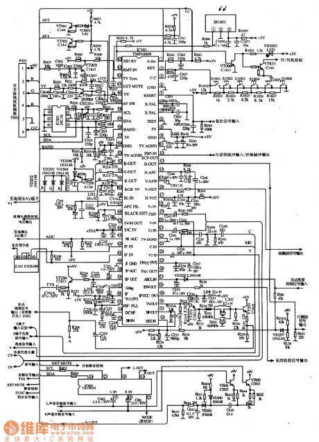
TypicalApplied Ciruict of IC TMPA8890
TMPA809 is a multi-function super-monolithic integrated circuit produced by Toshiba Corporation. It is used in domestic and imported color television set, such as Toshiba series large-screen color television set ,and Haier series large-screen color television set, as well as TCL series etc.
1 function features:
TMPA8809 integrated circuit includes control system micro computer circuit, TV signal processing, line scanning and field scanning small-signal processing circuit, teletext decorder circuit and some other auxiliary circuits.
2 function and feature of the pins
The pins of IC TMPA8809 adopt dual-in-line packages .
3 typical applied circuit
The above picture is a typical applied circuit diagram of TV signal processing and control system which is composed of TMPA8809 integrated circuit . (View)
View full Circuit Diagram | Comments | Reading(2634)
TMPA8807PSN Multi-Function Super Monolithic Circuit Diagram
Published:2011/7/3 2:38:00 Author:Vicky | Keyword: Multi-Function, Super Monolithic
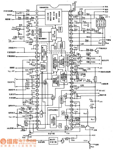
Internal Block Circuit Diagram and Typical Applied Circuit
TMPA8807PSN is a television multi-function super-monolithic integrated circuit produced by Toshiba Corporation. It is widely used in large-screen color television set of Kongka series, TCL series, Haier series, Toshiba series, Hisense Serires, and Changhong series etc.
1 functions and features
IC TMPA8807PSN includes microprocessor, television small-signal processing circuit, teletext decoder circuit and some other accessory functional circuit.
2 functions and datum of pins
ICPA8807PSN uses 64 pins which are in dual-in-line package. It is available in PAL, NTSC and SECAM.
3 typical applied circuit
The internal block circuit diagram and typical applied circuit is shown in the above picture.
(View)
View full Circuit Diagram | Comments | Reading(831)
Colour TV power supply controller circuit
Published:2011/3/30 1:28:00 Author:may | Keyword: Colour TV power supply controller
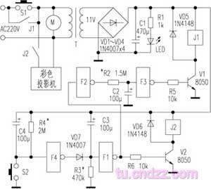
View full Circuit Diagram | Comments | Reading(1597)
Simple TV additional remote control circuit composed of LM555 and CD4017
Published:2011/3/27 22:05:00 Author:may | Keyword: TV additional remote control
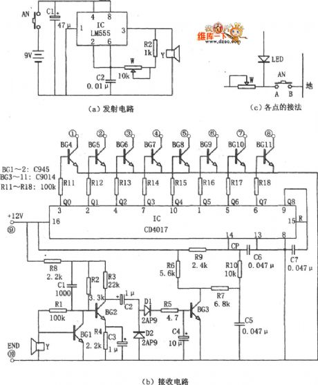
Simple TV additional remote control circuit composed of LM555 and CD4017 is shown in the diagram:
(View)
View full Circuit Diagram | Comments | Reading(1599)
TV LED electronic forceps monitoring circuit diagram
Published:2011/3/30 21:19:00 Author:Ecco | Keyword: TV, LED electronic forceps
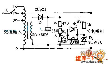
When the switch places(2), the output voltage is homology to input voltage, if the voltage were normal(200~240 V),both of two luminotrons couldn't be bright. When the voltage rises to 250 V, the rise of A electric potential will make red luminotron bright, when the switch places(2), then make output be 220V, the red luminotron again douses again. When Lou voltage drop arrived at 190 V, the green luminotron will be bright, the switch places(3).
(View)
View full Circuit Diagram | Comments | Reading(1388)
LCD TV power supply circuit diagram
Published:2011/3/27 20:34:00 Author:Rebekka | Keyword: LCD TV
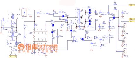
LCD TV power supply circuit diagram is shown as below.
(View)
View full Circuit Diagram | Comments | Reading(13959)
TV antenna principle circuit
Published:2011/3/21 2:56:00 Author:Joan | Keyword: TV antenna
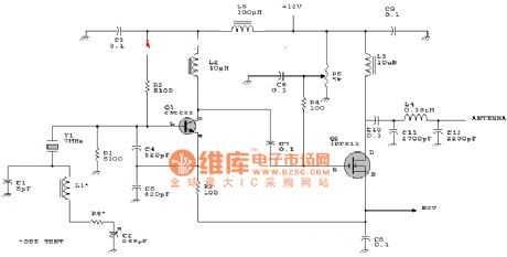
The figure is TV antenna principle circuit.
(View)
View full Circuit Diagram | Comments | Reading(4046)
| Pages:2/2 12 |
Circuit Categories
power supply circuit
Amplifier Circuit
Basic Circuit
LED and Light Circuit
Sensor Circuit
Signal Processing
Electrical Equipment Circuit
Control Circuit
Remote Control Circuit
A/D-D/A Converter Circuit
Audio Circuit
Measuring and Test Circuit
Communication Circuit
Computer-Related Circuit
555 Circuit
Automotive Circuit
Repairing Circuit