
Circuit Diagram
Index 1388
Photoelectric lighting circuit diagram
Published:2011/7/28 2:11:00 Author:Ecco | Keyword: Photoelectric lighting
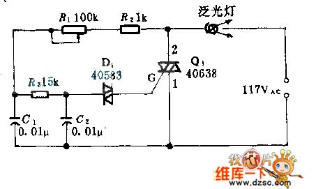
Influenced by bidirectional triode thyristor Q1 and disconnect rock, bidirectional switching LED D1, and potentiometer R1, the circuitry can connect 500w lamps, and the light could be turned on absolutely. Using a 5A rapid safety machine to connect lamps in series, it can avoid the current from breaking bidirectional Hiccup controlled silicon by the current at short circuit.
(View)
View full Circuit Diagram | Comments | Reading(978)
TELEPHONE_CIRCUIT
Published:2009/6/22 22:58:00 Author:May
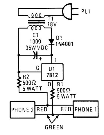
This circuit is useful for checking out old telephones by providing them with the dc voltage that they require for operation. (View)
View full Circuit Diagram | Comments | Reading(0)
The 555 linear PWM circuit
Published:2011/7/20 7:47:00 Author:Seven | Keyword: linear PWM circuit
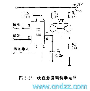
See as figure 5-25, IC(555), R2, VT1 and C1 compose the controllable single steady circuit, the contemporary pulse wavelength is in backward proportion to the input modulation signal, the higher the modulation LEV is, the narrower the pulse will be. VT1 is a symmetric dual triode BT51, which composes the mirror image current source with R2 and R3, and the mirror image makes the charge current of C1 keep linear in the contemporary stable period, the linearity is ±0.2%.
(View)
View full Circuit Diagram | Comments | Reading(1135)
KEY_WIRELESS_RTS_WITH_DATA
Published:2009/6/22 23:02:00 Author:Jessie
This simple keyer supplies both the RTS control and data delay needed to interface a digital ra-dio with an RS-232, data-only system. It supports speeds to 19.2 kbits/s sync or async. (View)
View full Circuit Diagram | Comments | Reading(1576)
SOLAR_POWER_SUPPLY_WITH_LINEAR_REGULATOR
Published:2009/6/22 22:58:00 Author:May
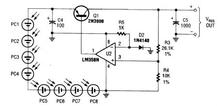
This regulator delivers a constant 2.4 Vdc for powering small devices that run on two AA cells, such as cassettes and small radios. Regulator drop is about 0.3 volt. This should be considered when choosing solar cells. Load current is typically 125 mA. (View)
View full Circuit Diagram | Comments | Reading(1900)
THERMOMETER_FOR_5_V_OPERATION
Published:2009/6/22 23:02:00 Author:Jessie
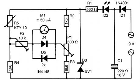
At the heart of this simple circuit is the well-known type KTY10 temperature sensor from Siemens. This silicon sensor is essentially a temp erature -dependent resistor that is connected as one arm in a bridge circuit here. Preset P1 functions to balance the bridge at 0℃. At that temperature, moving coil meter M1 should not deflect, i.e., the needle is in the center position. Temperature vari-ations cause the bridge to be unbalanced, and hence produce a proportional indication on the meter. Calibration at, say, 20℃ is carried out with the aid of P2.The bridge is fed from a stabilized 5.1-V supply, based on a temperature-compensated zener-diode. It is also possible to feed the thermometer from a 9-V battery, provided D1-D3, R1 and C1 are replaced with a Type 78L05 voltage regulator, because this is more economic as regards to current c onsumption. (View)
View full Circuit Diagram | Comments | Reading(2179)
TELEPHONE_HOLD_CIRCUIT
Published:2009/6/22 22:57:00 Author:May
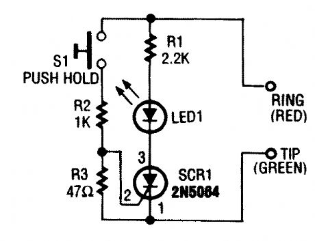
When S1 is pressed, the SCR fires, and places LED1 and R1 across the phone line. The line volt-age drops to about 20 V, which holds the connec-tion to the phone company's central office. (View)
View full Circuit Diagram | Comments | Reading(0)
VIDEO,POWER,AND_CHANNEL_SELECT_SIGNAL_CARRIER
Published:2009/6/22 23:01:00 Author:Jessie

In the video system of Figs. A and B, a single coaxial cable carries power to the remote location, selects one of eight video channels, and returns the selected signal. The system can choose one of several remote surveillance-camera signals, for example, and display the picture on a monitor near the interface box.
The heart of the multiplexer box (A) is a combination 8-channel rnultiplexer and amplifier (ICl). C11 couples the multiplexer's baseband video output to the coax, and L1 decouples the video from dc power arriving on the same line. This power-approximately 30 mA at 10 V-supplies all circuitry in the multiplexer box.
In interface box (B), a desired channel is encoded by three bits, set either by switches as shown or by an applied digital input. Momentary depression of the send button triggers clownconverter IC1 and gated oscillator IC2A to initiate a channel-selection burst. (View)
View full Circuit Diagram | Comments | Reading(2334)
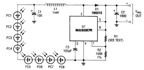
RECHARGEABLE_SOLAR_POWER_FOR_SUN_TRACKER
Published:2009/6/22 23:01:00 Author:Jessie
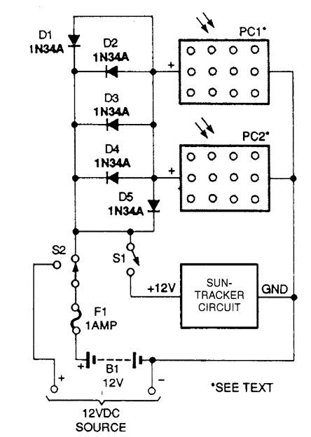
This application circuit provides rechargeable solar power for the sun tracker, as well as for another 12-volt device. PC1 and PC2 can be mounted on sun tracker assembly. (View)
View full Circuit Diagram | Comments | Reading(0)
MOSFET_DRIVE_CURRENT_BOOSTER
Published:2009/6/22 23:01:00 Author:Jessie
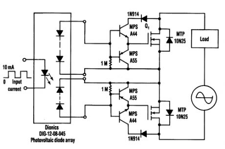

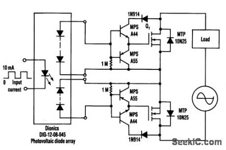
A clean and inexpensive way to eliminate the floating-gate supply is to use the voltage available at the MOSFET's drain to drive its gate. Tying the collector of Q1(a high-voltage, small-signal, 400-V NPN)to the MOSFET's drain supplies sufficient gate-drive voltage when it's needed most-when the MOSFET's drain-to-source voltage is high. Two such circuits used back-to-back form an ac relay.Using the emitter follower attached to the drain increases gate-drive current and decreases the MOSFET's turn-on time by a factor equal to the high-voltage NPN's beta. The resulting drain-to-source voltage fall times depend on the MOSFET's size and its required gate charge. The circuit that's used gives a fall time of 200 ps for an MTP10N2f5 10-A, 250-V MOSFET. With such fall times cutting switching losses, pulse-width modulation at frequencies under 100 Hz is possible.During tune-on, VDS falls rapidly until it reaches the sum of the 1N914 diode's 0.7-V drop, the collector-emitter saturation voltage of Q1, and the gate-to-source voltage required to support the load cur-rent. At that point, the diode array completes the MOSFET's turn-on, unaided by the buffer. This slows the fall of 7,s considerably when it reaches about 5 to 7 V. In high-voltage, low-frequency systems, tail-'ma of VDS is tolerable because the tail's voltage magnitude constitutes a small fraction of the switching voltage. The IN914 makes it possible for VGS to exceed VDS as the MOSFET completes turn-on. (View)
View full Circuit Diagram | Comments | Reading(3461)
PG_PASSWORD_PROTECTOR
Published:2009/6/22 23:01:00 Author:Jessie
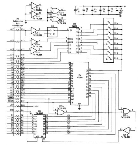
IC4, a static RAM, is mounted in a smart built-in switch over circuitry. This retains SRAM con-tents when power is off. The rest of the circuitry consists of address decoding logic and jumper JU1, used to decode a 16K address space for the 32K static RAM. Software is necessary and this is con-tained in the original article (see reference). (View)
View full Circuit Diagram | Comments | Reading(1900)
The internal circuit diagram of crystal triodes EMG1,UMG1N
Published:2011/7/21 3:08:00 Author:Ecco | Keyword: crystal triodes, internal circuit
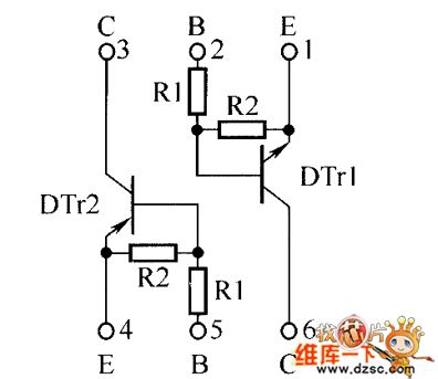
The internal circuit diagram of crystal triode EMG1,UMG1N is as below:
(View)
View full Circuit Diagram | Comments | Reading(469)
TEMPERATURE_COMPENSATION_ADJUSTER
Published:2009/6/22 23:01:00 Author:Jessie
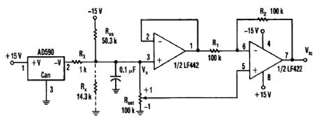
The circuit shown delivers +10 to -10 mV°/C output using an Analog Devices' AD590 temperature transducer. Rx is a scaling resistor. (View)
View full Circuit Diagram | Comments | Reading(1211)
SOLAR_POWER_SUPPLY
Published:2009/6/22 22:57:00 Author:May
This circuit delivers either 4.8 or 7.2 V regulated at 15 mA with a 3-V input from a bank of pho-tocells. R1 should be 453 kΩ for a 7.2-V output and 274 kΩ for a 4.8-Vdc output. Regulator efficiency is around 70%. This should be considered when selecting suitable solar cells. (View)
View full Circuit Diagram | Comments | Reading(800)
PHOTODIODE_LOG_CONVERTER_TRA_NSMITTER
Published:2009/6/22 23:00:00 Author:Jessie

A logarithmic conversion is made on the output current of a photodiode to compress a fourdecade, light-intensity variation into a standard transmission range. The circuit is balanced at midrange, where R3 should be chosen so that the current through it equals the photodiode current. The log-conversion slope is temperature compensated with R6. Setting the reference output to 1.22 V gives a current through R2 that is proportional to absolute temperature because of D1 so that this level-shift voltage matches the temperature coefficient of R6. C1 has been added so that large-area photodiodes with high capacitance do not cause frequency instabilities. (View)
View full Circuit Diagram | Comments | Reading(1383)
TELEPHONE_AMPLIFIER
Published:2009/6/22 22:57:00 Author:May
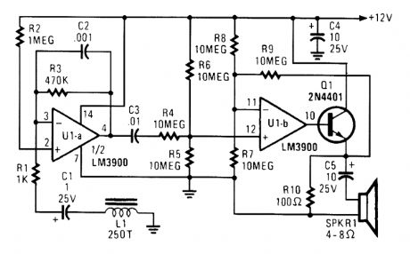
Section UI-a is configured as a high-gain inverting voltage amplifier that is inductively coupled to the phone line via L1. Inductor L1 is a homemade unit that consists of 250 turns of fine, enamel-coated wire that is wound on an iron core. The op amp receives the few mV produced by L1 via C1 and RI and amplifies the signal. Capacitor C1 acts as the negative-feedback component that limits the circuit's high-frequency gain, while R3 limits the low-frequency gain. Resistor R3 is particularly important because without it, the amplifier would saturate.Op amp UI-b is configured as a difference amplifier. It receives a signal from U1-a via C3 and R4 and amplifies the difference between it and half of the supply voltage. Transistor Q1 is configured as a common-collector amplifier ensuring sufficient signal to drive the speaker. Capacitor C5 is used to remove any dc component provided by transistor Q1. (View)
View full Circuit Diagram | Comments | Reading(1897)
TELEPHONE_LINE_TESTER
Published:2009/6/22 22:59:00 Author:Jessie
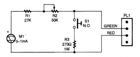
The telephone-line tester consists of nothing more than a meter (that's used to measure line voltage in the on- and off-hook state), three resistors (one of which is variable), a pushbutton switch, and a modular telephone connector. When the circuit is connected to the telephone line, a meter reading of 5 to 10 V (when S1 is pressed) indicates that the line is okay. (View)
View full Circuit Diagram | Comments | Reading(2604)
MOSFET high frequency amplifier circuit diagram
Published:2011/3/30 22:20:00 Author:Ecco | Keyword: high frequency amplifier
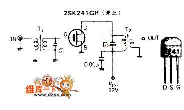
The preamplifier(1) VHF high frequency amplifier circuit of unipole gate polar MOS FET is based on Bipolar Transistor, but mostly replaced by the FET now. Figure 2-1 is its typical circuitry, 2SK241(Toshiba) adopts FET to increase its gaining power to 28dB(@100MHz). And it is suitable for VHF receiver to amplifier its frequency class. As been zero bias on operating point, the structure of the circuitry is simple, the whole components is 6. Figure 2-1shows a inductance and capacitance which can apply in different kinds of high frequency amplifiers. When the polar current is 9mA, the current will keep constant with the voltage in the range of 6~12V.
(View)
View full Circuit Diagram | Comments | Reading(3277)
LED_LIGHTWAVE_RECEIVER
Published:2009/6/22 22:56:00 Author:May
View full Circuit Diagram | Comments | Reading(799)
TELEPHONE_CIRCUIT
Published:2009/6/22 22:58:00 Author:Jessie
This circuit is useful for checking out old telephones by providing them with the dc voltage that they require for operation. (View)
View full Circuit Diagram | Comments | Reading(1695)
| Pages:1388/2234 At 2013811382138313841385138613871388138913901391139213931394139513961397139813991400Under 20 |
Circuit Categories
power supply circuit
Amplifier Circuit
Basic Circuit
LED and Light Circuit
Sensor Circuit
Signal Processing
Electrical Equipment Circuit
Control Circuit
Remote Control Circuit
A/D-D/A Converter Circuit
Audio Circuit
Measuring and Test Circuit
Communication Circuit
Computer-Related Circuit
555 Circuit
Automotive Circuit
Repairing Circuit