
Circuit Diagram
Index 465
Automatic interval timer circuit composed of PUT
Published:2011/9/13 2:04:00 Author:Rebekka | Keyword: Automatic interval timer
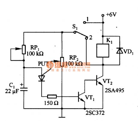
Figure 1 is composed of the PUT and other automatic interval timer circuit. In the circuit, PUT is the oscillator. Using the switch S1 to switchover the interval time and automatic time. When S1 connects to 1, it is automatic timing mode 1, thenS1connects to2, itis the interval time. If the resistance of RP2is too large, PUT anode current is less than the maintenance current, the circuit can not be used as the automatic timing circuit. (View)
View full Circuit Diagram | Comments | Reading(2324)
The time delay circuit diagram composed of transistor
Published:2011/9/13 1:51:00 Author:Rebekka | Keyword: transistor , time delay
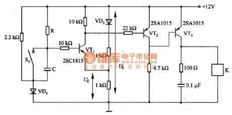

(a) Timedelay circuit
(b) Timedelay circuit
It can set delay time according to the voltage Us and resistor R. In the circuit, S1 is the the discharge switch of capacitor C. When the switch S1 is closed, the stored charge on C will be released through S1 to ensure the accuracy of the delay time the next time. VD1 and VD2 are used to eliminate the impact of VT1 by its voltage UBE. In the circuit, the load current can be only 5OnA. If VT3 is replaced by Darlington transistor, the load current will be increased. VT1 uses 2SC1815; VT2 and VT3 use 2SAlO15; VD1 and VD2 use 1S1588. Delay time T = RC1n1 / (1-K), K = Uc / Us. Figure 1 (b) is a time delay circuit composedof the transistor and the comparator. It is similar with the circuit shown in Figure 1(a). The comparison circuit uses comparator integrated chip M51206L. It is not effected by environmental temperature and supply voltage variations. Therefore, the circuit is very stable. If VT2 uses the Darlington power transistor, you can drive higher current load.
(View)
View full Circuit Diagram | Comments | Reading(3317)
Mitsubishi Pajero light off-road vehicle body circuit body cable configuration circuit diagram
Published:2011/8/31 2:27:00 Author:Rebekka | Keyword: Mitsubishi Pajero, light off-road vehicle , body cable configuration
01.02-rear speakers (left); 03 - door switch (right); 04 - room light; 06.07-rear speakers (right); 14 - rear integrated light; 16 - tail light (right); 17.18.19.20-license plate lights; 21 - tail light (left); 23 - fuel gauge device; 24 - the front wiring processing and frame processing; 26 - front door switch (left) 37 - Front power windows motor (right); 38 - front power deputy window switch; 39.40-sun hood switch; 41 - back door before the wiring wiring wiring wiring processing and integrated treatment; 42 - Deputy Mayor after the power window switches; 43 - big rear door lock motors; 44 - Cargo room lamp; 45 - back door switch; 46 - frame wiring process and large rear door handle; 47 - Frame wiring dealing and side wiring processing synthesis (right); 48 - big moverear door lock motor; 49 - frame wiring and side wiring dealing processing synthesis (left); 50 - back door switch (left), 51 -back power window motor (left); 52 - back vice-switch power windows (left); 53 - front wiring connection line treatment and back wiring connection comprehensive treatment (left); 54 - fromt power window main switch; 55 - front power window motor (right). (View)
View full Circuit Diagram | Comments | Reading(4673)
The boost converter circuit diagram composed of LTC3401
Published:2011/8/31 2:20:00 Author:Rebekka | Keyword: boost converter
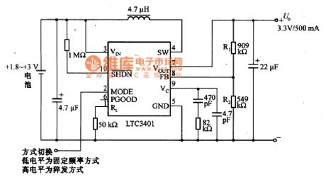
Boost converter circuit is composed of LTC3401. LTC3401 is a circuit which has all the functions needed by boost power supply. it can start to work with 1V input voltage. It costs a low current with38μA. Input voltage range is 1 ~ 5V, output voltage is set in 2.6 ~ 5Vby R1 and R2. LTC3401 uses 2-pin mode switching terminal. The control signal can be applied. When the control signal is low, LTC3401 works for the fixed frequency. Ituses burst working mode when the level is high. (View)
View full Circuit Diagram | Comments | Reading(1120)
The buck converter circuit diagram composed of LM305
Published:2011/8/31 2:15:00 Author:Rebekka | Keyword: buck converter
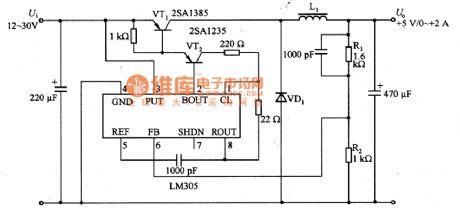
The buck converter circuit is composed of LM305. It uses self-excited buck DC / DC converter. Input voltage is +12 ~ +30 V, output voltage is +5 V, maximum output current is 2A. The internal LM3O5 is a robot control integrated circuit composed of a reference voltage, operational amplifiers, driver circuit. Output voltage is set to 3V or less. It can not be switching. The loss of VT increases. Output voltage U. = [(R1 + R2/R2] UREF, UREF = 1.8V. (View)
View full Circuit Diagram | Comments | Reading(3683)
Mitsubishi Pajero light off-road vehicle circuit dashboard wiring circuit diagram
Published:2011/8/31 2:07:00 Author:Rebekka | Keyword: Mitsubishi Pajero , light off-road vehicle , dashboard wiring
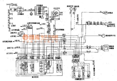
View full Circuit Diagram | Comments | Reading(4571)
Mitsubishi Pajero (PAJERO) brand light off-road vehicle lighting and signal principle circuit diagram
Published:2011/8/31 2:06:00 Author:Rebekka | Keyword: Mitsubishi Pajero (PAJERO) , light off-road vehicle
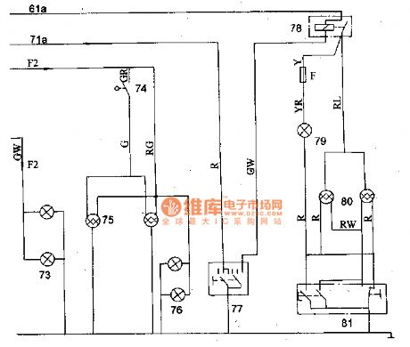
61- fusible wire; 71a-meter relay; 73- license plate lamp light; 74- reversing light switch; 75- reversing light, tail light; 76- width light; 77- light switch; 78-headlamp relay;79- beam; 80- headlamp; 81-overtaking and dimmer switch. (View)
View full Circuit Diagram | Comments | Reading(986)
Mitsubishi Pajero (PAJERO) brand light off-road vehicle lighting principle circuit diagram
Published:2011/8/31 2:03:00 Author:Rebekka | Keyword: Mitsubishi Pajero (PAJERO) , light off-road vehicle, lighting principle
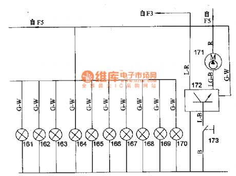
161-instrument lights; 162- lights that cigarette smoke; 163- ashtray light; 164- defroster switch lights; 165- automatic antenna switch forheadlamp; 166- electronic compass lights; 167,168- air conditioning controller light, 169,167- the backblower switch lights; 171-headlight washing motor; 172- forheadlamp washer relay; 173- forheadlamp washing switch.
(View)
View full Circuit Diagram | Comments | Reading(1013)
Electric fence control circuit 6
Published:2011/8/1 3:03:00 Author:Ecco | Keyword: Electric fence control
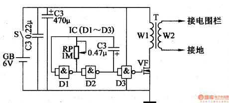
The electric fence control circuit is composed of the power supply circuit, oscillator and pulse voltage output circuit, and it is shown in Figure 4-31. Power supply circuit is composed of the battery GB, power switch S and capacitors Cl, C2. Oscillator is composed of the NAND gates Dl, D2 which are inside of NAND gate IC (Dl-D3 are connected as the NOT gate) and potentiometer RP, capacitor C3. Pulse voltage output circuit is composed of the internal D3 of IC NAND gate, field-effect transistor VF and pulse transformer T.
(View)
View full Circuit Diagram | Comments | Reading(2527)
Mitsubishi Pajero light off-road car dashboard ( vehicles without electronic compasses) wiring circuit diagram
Published:2011/8/31 1:58:00 Author:Rebekka | Keyword: Mitsubishi Pajero , light off-road car dashboard, electronic compasses, wiring circuit
View full Circuit Diagram | Comments | Reading(2868)
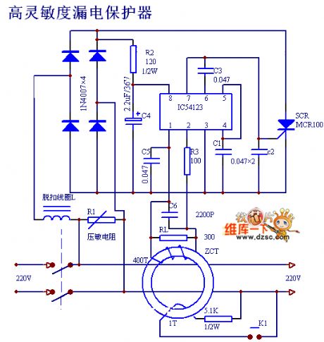
High sensitivity leakage protector circuit diagram
Published:2011/9/14 22:10:00 Author:Rebekka | Keyword: Leakage protection, leakage protector
View full Circuit Diagram | Comments | Reading(1348)
Motorcycle charging circuit diagram
Published:2011/9/14 22:16:00 Author:Rebekka | Keyword: Motorcycle charging
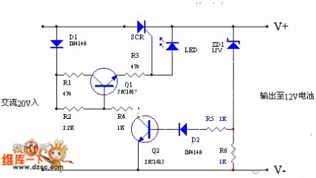
The circuit uses ACpositive half cycle charge. Charging speed is fast and it can extend battery life. People use the charger on ordinary motorcycle. It has an excellent performance and saves 5% fuel. It is a practical charging circuit. Working principle: (shown as the figure)AC voltage is also added to the D1 and SCR. It passes the half-wave rectifier D1 to R1、R2、Q1、R3 and provides trigger voltage to SCR. SCR is charging to the battery at this time. When the battery voltage isup to 13.5V, the ZD1 will be conducted. The voltage passing R5、D2 provides bias to Q2, thenQ2 will be conducted. Q1 reverse bias will be closed. SCR stops outputting when battery voltage is lower than 13-13.5V.
(View)
View full Circuit Diagram | Comments | Reading(6284)
AM synchronous detection circuit diagram
Published:2011/9/14 22:37:00 Author:Rebekka | Keyword: AM synchronous detection circuit
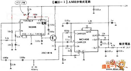
For wide range input signal level, it needs to use the synchronous detection circuit shown in the figure 16-1 if you want to get linear detector output. First it uses PLLICNE565 to make a moving signal that is the same with input signal n/2. Then it uses multiplier ICMC1496 and phase shift signalling to switch the input signal. After full-wave rectification, it can get detected output signal, moreover, because the rectification action works with input signal, the detected circuit has frequency selectivity.
(View)
View full Circuit Diagram | Comments | Reading(4063)
Light audio controlling touching circuit diagram
Published:2011/9/14 22:23:00 Author:Rebekka | Keyword: Light , audio controlling touching
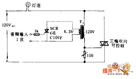
Three-terminal two-way SCRis controlled bylampon - off set. Two-way SCR is triggered by 1v audio signal. T1 is an isolation transformer. Since the action of switching is much faster than the reaction of light bulbs and the human eyes. The effect of the audio control is similar to the proportional control. When resistor R1 is set to the maximum input is zero. But bulb can not do that. Three-terminal two-way SCR should match to the bulb.
(View)
View full Circuit Diagram | Comments | Reading(913)
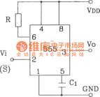
Indirect self-excited feedback astable multivibrator circuit composed of 555
Published:2011/8/23 21:10:00 Author:Ecco | Keyword: Indirect self-excited feedback , astable multivibrator , 555
View full Circuit Diagram | Comments | Reading(741)
Single-end bistable circuit composed of 555
Published:2011/8/23 21:10:00 Author:Ecco | Keyword: Single-end , bistable circuit , 555
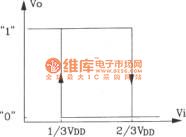
(View)
View full Circuit Diagram | Comments | Reading(1076)
555 simple refrigerator protection circuit
Published:2011/8/2 1:16:00 Author:Ecco | Keyword: 555, simple , refrigerator, protection
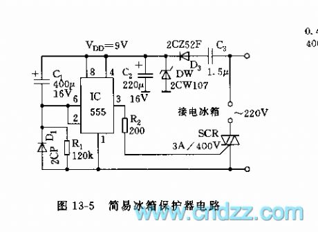
The circuit is shown in Figure 13-5, the protection is mainly used for power delay protection to avoid the compressor from frequent start, and mechanical damage from the non-equilibrium state. When it stops, the voltage on C1 discharges through D1 immediately. When it gets power again, because the voltage on C1 is not mutation, 555 is in the reseting state; until C1 is charged to td = 1.1R1C1, which is about 6 minutes, 2 foot level is below the 1/3 VDD, 555 is set, the SCR then is connected, refrigerator is running.
(View)
View full Circuit Diagram | Comments | Reading(3208)
555 Automatic fan speed controller circuit
Published:2011/8/4 22:00:00 Author:Ecco | Keyword: 555 , Automatic, fan speed , controller
As shown in Figure 12-9, the controller circuit consists of step-down rectifier circuit and an oscillator and control circuit. 555 and R2, RP1, C3 and thermistor RT form a non-steady multivibrator, the oscillation frequency f = 1.44 / (R2 + RP1 +2 RT) C3. It can be shown by the formula, the oscillation frequency is related to RT. When it selects a negative temperature coefficient thermistor, the temperature rises, RT resistance decreases, the oscillation frequency increases, and the duty cycle increases, the motor conduction timeincreases, natural wind increases; or the temperature drops, the power-on time reduces, the natural wind is weaken.
(View)
View full Circuit Diagram | Comments | Reading(3573)
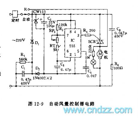
555 Ventilator automatic timing controller circuit
Published:2011/8/4 21:58:00 Author:Ecco | Keyword: 555 , Ventilator, automatic timing , controller
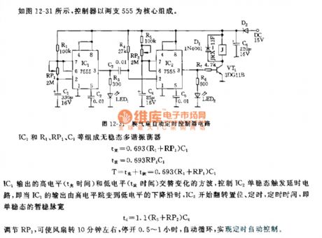
The controller shown as figure 12-31 is based on two roads of 555. IC1 and R1, PR1, C1 etc. form astable multivibrator. IC1 outputs alternating high and low output square wave to control the trigger IC2 monostable delay circuit, that is, when falling delay of IC1's output changes from high to low level, IC2 starts flipping set, timing.Adjusting RP2 can turn onthe fan for about 10 minutes and close 0.5 to 1 hour, it will change in automatic cycle to achieve automatic control of time.
(View)
View full Circuit Diagram | Comments | Reading(1560)
555 voice circuit in fencing
Published:2011/8/4 21:57:00 Author:Ecco | Keyword: 555 , voice circuit , fencing
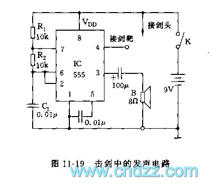
The circuit is shown as figure 11-19, 555 is the core of the circuit. The pin 4 of 555 is the reset terminal, when the voltage is below 0.7V, then the shock ends. The leading wire of pin 4 is connected to metal arrow, if hitting the target is connected to the power (higher than 1.4V) in the game, the 555 circuit will shock, vibration frequency depends on R1, R2, C1's value, that is, f = 1.44 (R1 +2 R2) C1. icon parameter frequency is about 800Hz, if hitting, it will emit sound. If tipis away from the target, the circuit is forced to be in reset state.
(View)
View full Circuit Diagram | Comments | Reading(1365)
| Pages:465/2234 At 20461462463464465466467468469470471472473474475476477478479480Under 20 |
Circuit Categories
power supply circuit
Amplifier Circuit
Basic Circuit
LED and Light Circuit
Sensor Circuit
Signal Processing
Electrical Equipment Circuit
Control Circuit
Remote Control Circuit
A/D-D/A Converter Circuit
Audio Circuit
Measuring and Test Circuit
Communication Circuit
Computer-Related Circuit
555 Circuit
Automotive Circuit
Repairing Circuit