
Circuit Diagram
Index 461
Cadillac anti-theft circuit diagram
Published:2011/9/15 2:18:00 Author:Rebekka | Keyword: Cadillac , anti-theft
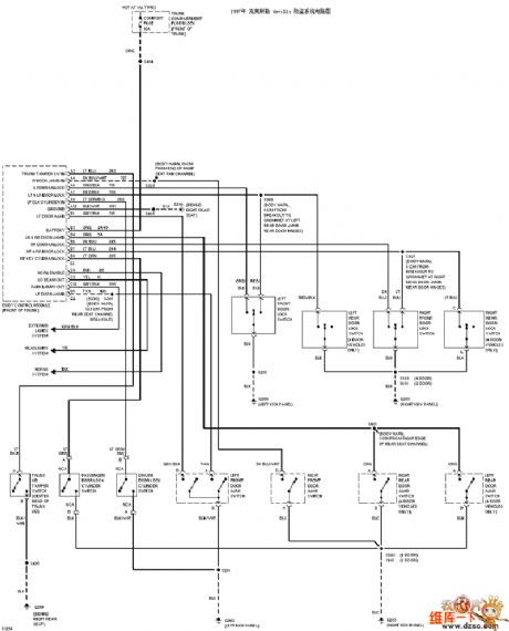
View full Circuit Diagram | Comments | Reading(775)
Chang an Star air conditioning system data circuit diagram
Published:2011/9/15 2:18:00 Author:Rebekka | Keyword: Chang an Star, air conditioning system data
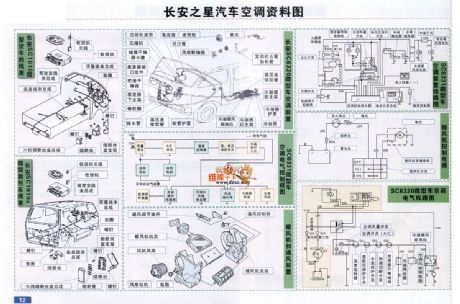
View full Circuit Diagram | Comments | Reading(970)
Cadillac electronic suspension circuit diagram
Published:2011/9/15 2:19:00 Author:Rebekka | Keyword: Cadillac , electronic suspension
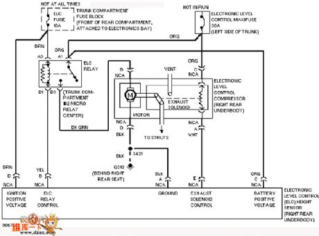
View full Circuit Diagram | Comments | Reading(1209)
Cadillac electrothermal rearview mirror circuit diagram
Published:2011/9/15 2:19:00 Author:Rebekka | Keyword: Cadillac , electrothermal rearview mirror
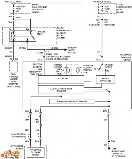
View full Circuit Diagram | Comments | Reading(721)
Cadillac cooling fan circuit diagram
Published:2011/9/15 21:14:00 Author:Rebekka | Keyword: Cadillac , Cooling fan
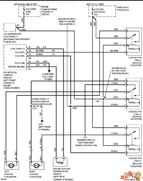
View full Circuit Diagram | Comments | Reading(918)
Missing pulse alarm circuit diagram
Published:2011/9/15 1:56:00 Author:Rebekka | Keyword: Missing pulse alarm
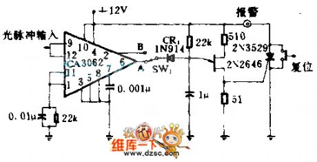
The circuit is used to detect the missing optical pulse or shortage of goods on the conveyor belt. CA3062 combination of detectors and amplifier can detect optical pulse which is synchronous with 60HZ power frequency . When switch SW1 is at A, every pulse has a interval of 16.7ms. It makes 2N2646 unijunction transistor reset at 20ms timing network. It avoids unijunction transistor triggering and triggers controlled rectifier. The alarm will be connected. When the SW1 at B, the circuit stops the detection of steady-state beam. It only alarmsat uninterrupted time.
(View)
View full Circuit Diagram | Comments | Reading(1487)
LG PT-48A82 Rear projection TV power supply circuit diagram
Published:2011/9/15 1:56:00 Author:Rebekka | Keyword: Rear Projection TV
View full Circuit Diagram | Comments | Reading(8252)
Water tank water level alarm circuit diagram
Published:2011/9/15 2:04:00 Author:Rebekka | Keyword: Water tank water level alarm
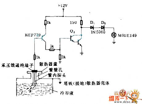
The insulator is stalledinto the lid of water tank. The insulator should suffer 0.717X10⁻⁴kg/m2 pressure from water tank. Metal probe passing the insulator is put into the liquid of water tank in the high temperature tube. There is small holes near to the one end of water tank lid. It can make the liquid rise in the tube and reach the probe. When the water level falls lower than the probe, the collector potancial of clad pipe Q2 rises and turns on the diode. The alarm M1 light will be lit. (View)
View full Circuit Diagram | Comments | Reading(2243)
MAG Long 796FDⅡtype color display switching power supply (UC3842) circuit diagram
Published:2011/9/15 1:57:00 Author:Rebekka | Keyword: MAG Long , color display switching
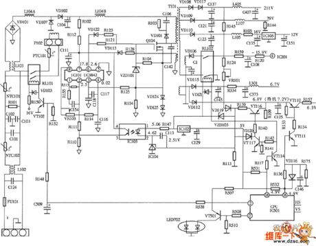
View full Circuit Diagram | Comments | Reading(4520)
Photoelectric encoder circuit diagram
Published:2011/9/15 1:23:00 Author:Rebekka | Keyword: photoelectric encoder
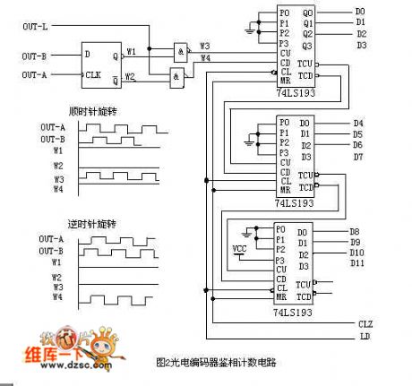
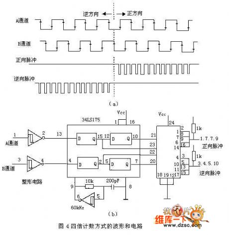
In the angle measurement, displacement measurement, it has a strong anti-interference ability and a stable and reliable output pulse signal. And after the pulse signal obtained by counting, the number of signals can be measured. Therefore, when we develope driving simulator for the steering wheel rotation angle measurement, we use EPC-755A optical encoder as the sensor. The outgoing circuit selects an open-collector. The output resolution selects 360 pulse / cycle. It needs the encoder output signal phase before counting.
D flip-flop outputing Q (waveform W1) is high, Q (waveform W2) is low. It is sent to counter 74LS193 bi-directional, then thepulse is input plus CU to plus count; At this point, the following NAND gate is closed, the output is high (waveform W4).
(View)
View full Circuit Diagram | Comments | Reading(2920)
The logic circuit diagram composed of photocoupler
Published:2011/9/15 1:21:00 Author:Rebekka | Keyword: photocoupler , logic circuit
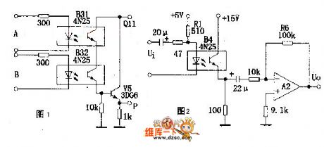
Figure 1 is AND gate logic circuit. Its logic expression is P=A, Figure B has 2 photodiodes in series. When input logic level A=1, B=1, output P=1. In a similar way, itcan form Or gate , NAND gate , NOR gate and some other logic circuits.
As shown in figure 2, it is a typical AC coupling amplifier circuit, which is suitable for selecting lighting loop SFCL Rl to make B4's current transmission be a constant and protect the linear amplifier effect of the circuit. (View)
View full Circuit Diagram | Comments | Reading(1869)
The circuit of logic probe with memories
Published:2011/9/15 1:17:00 Author:Rebekka | Keyword: logic probe with memories
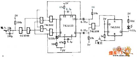
The circuit can be used for camera jitter detection. It is suitable for ±15V input signal. When the probe inputs 1, the negative trigger terminal of dual monostable circuit 74LS123 is in low level, light LED1 is lit, when the input falls down, 9 will be triggered and 5 has a transition. LED1 shows 20ms dark time. When the input is 0, LED 2 is dark, but the positive jump will make LED1 show 20ms light schedule. The 13 and 5 of 74LS123 have the function of memory. (View)
View full Circuit Diagram | Comments | Reading(2172)
Optical coupling circuit for bistable output
Published:2011/9/26 1:41:00 Author:Rebekka | Keyword: bistable output , optical coupling circuit

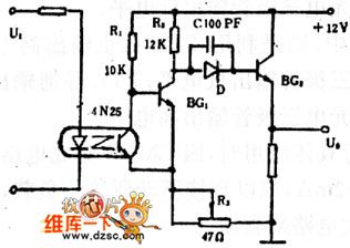
Figure (a) shows the circuit of the control of bistable optical coupler output switch circuit, which is characterized by coupling the optical switch connected to the two emitter back on the road. It can effectively solve the isolate the problem between the output and load.
Graph (b) shows the circuit for the optical coupling switch Schmitt circuit. When the input voltage U1 is low, the optical transistor C and e are in high resistance, BG1 will be conducted, BG2 stops, the output voltage U0 is low; when the amplitude of the input voltage U1 is greater than amplitude discrimination value, the optical transistor c and e are in low resistance, the BG1 stops, BG2 will be conducted, the output U0 is high voltage. You can change the level of amplitude discrimination by adjusting resistor R3.
(View)
View full Circuit Diagram | Comments | Reading(980)
Photocoupler high voltage regulator circuit diagram
Published:2011/9/26 1:34:00 Author:Rebekka | Keyword: photocoupler, high voltage regulator
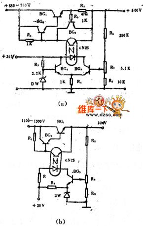
It is the series regulator circuit, and the amplifier tubes need to use relatively high-voltage transistor, if it uses the good insulation characteristics of optical coupler between input and output, it will realize high-pressure control. In the (a) and (b) figures, they are the high-voltage regulator circuit with using optocoupler. In Figure (a), when the output voltage rises for some reason, the BG5 bias increases, light-emitting diode's forward current increases, so that the phototransistor collector junction voltage decreases. (View)
View full Circuit Diagram | Comments | Reading(2398)
Optocoupler switch circuit diagram
Published:2011/9/15 2:12:00 Author:Rebekka | Keyword: Optocoupler switch
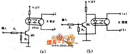
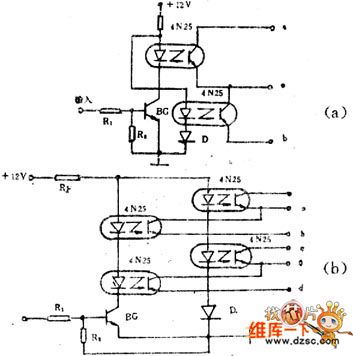
Figure 1 (b) shows off mode of the circuit. As no signal input, BG is stopped. When a signal is input, BG is conducted, due to BG's collector junction drops below 0.3V, which is much smaller than the light-emitting diode forward voltage, the light-emitting diode does not emit light without current flowing, then the resistance of a, b is large. It is equivalent to switch off . It is normally closed type. Visible, a, b ends are not limited by high or low potential in the circuit, but in theapplicationsof the circuit, we should make abe positive, b endbe negative, and U & ab> 3V, at the same time, Uab should be less than the BVceo of optical transistor.
(View)
View full Circuit Diagram | Comments | Reading(1325)
AC load control connector circuit diagram
Published:2011/9/15 2:08:00 Author:Rebekka | Keyword: AC load control connector
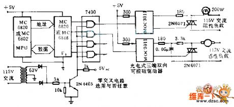
MC6820 external interface adapter can drive 4 dispersion gate 7400. The output signal is output by 7400 feeds back to MOC 3011 optical isolator. It controls three-terminal TRIAC, thenSCR cancontrol AC resistive load or AC inductive load. The second input end of NAND gate is connected to atransistorin 7400. The SCR will be turned on when AC input voltage crosses zero point. This way can last the life of incandescent longer and shorten the attackfrom surge current to three-terminal TRIAC. (View)
View full Circuit Diagram | Comments | Reading(1227)
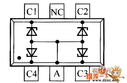
Crystal diode QZX3636C5V6 internal circuit diagram
Published:2011/9/15 2:04:00 Author:Rebekka | Keyword: Crystal diode, internal circuit
View full Circuit Diagram | Comments | Reading(857)
220v led indicator light circuit diagram
Published:2011/9/14 22:40:00 Author:Rebekka | Keyword: led indicator light
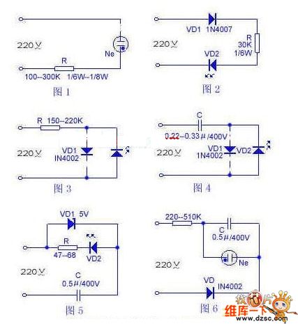
Figure 1 shows the circuit, whichhas only two components. R selects 1/6--1/8W carbon resister or metal film resistor, the resistance is betweenthe 1 - 300K. Ne is a neon bulb. It also uses the neon bulb in ordinary fluorescent starter. If you want to use 60V small neon bulb that is able to start neon bulb. The model is NNH-616 type, resistor R uses 270K 1 / 6W metal film resistor. Led light circuit is shown as the chart.
(View)
View full Circuit Diagram | Comments | Reading(14469)
CXA1019S frequency regulation amplitude modulation radio circuit diagram
Published:2011/9/14 22:38:00 Author:Rebekka | Keyword: frequency regulation, amplitude modulation
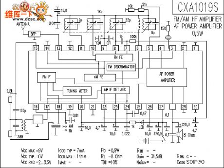
CXA1019 is Japanese SONY company'shigh-performance, high-sensitivity dedicated FM radio Manifold AM. CXA1019 high integration includes FM / AM tuner circuit, mixer circuit, squelch circuit, power amplifier (power is between0.5 ~ 1W), DC voltage control volume, instructions and other tuned circuit. It can complete all the basic functions of the radio. Because of its low cost, superior performance, it is widely used in a variety of portable radios and electronic products.
(View)
View full Circuit Diagram | Comments | Reading(8536)
485 and 75176 communications circuit diagram
Published:2011/9/15 1:53:00 Author:Rebekka | Keyword: communications circuit
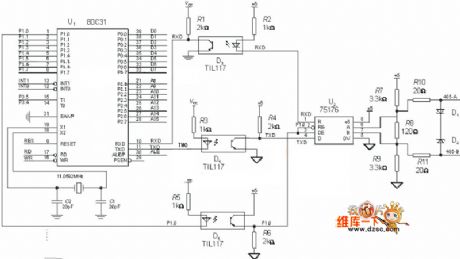
View full Circuit Diagram | Comments | Reading(12724)
| Pages:461/2234 At 20461462463464465466467468469470471472473474475476477478479480Under 20 |
Circuit Categories
power supply circuit
Amplifier Circuit
Basic Circuit
LED and Light Circuit
Sensor Circuit
Signal Processing
Electrical Equipment Circuit
Control Circuit
Remote Control Circuit
A/D-D/A Converter Circuit
Audio Circuit
Measuring and Test Circuit
Communication Circuit
Computer-Related Circuit
555 Circuit
Automotive Circuit
Repairing Circuit