
Circuit Diagram
Index 480
Single or dual power quad op-amp with high input impedance circuit
Published:2011/9/14 21:01:00 Author:John | Keyword: Single or dual power quad op-amp
CF14753 is classified into CMOS operational amplifiers. It has four high-performance op-map modules, which is quite similar to MC14753. It is equiped with phase compensation device inside. It is mainly used for a variety of analog computing circuits, AC amplifiers, low frequency waveform generators and active filters and so on. It can also be composed of chopper amplifiers and automatic zero op-amp. Substitutions or direct models are CFl4573, 5G14573, MCl4573, CHl4573 and CAl4573 and so forth.
(View)
View full Circuit Diagram | Comments | Reading(1236)
signal amplitude comparison circuit
Published:2011/9/14 19:49:00 Author:Nancy | Keyword: signal amplitude
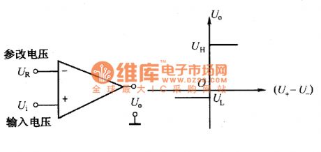
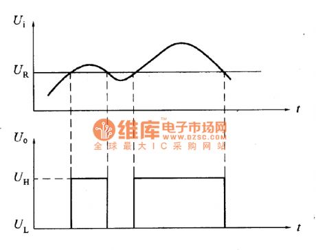
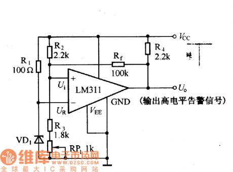
The figure shown is computer power test circuit, which uses LM311 integrated voltage comparator.When the power supply voltage VCC is low, it can output alarm signal, which causes the computer to take immediate processing measure to protect the data. The reference voltage UR in the circuit is decided by the value of voltage-regulator diode VD1, and can choose different voltage values according to the need. The input voltage Ui of the comparator is decided by the voltage division of R2, R3 and RP1, which is proportional to the Vcc supply voltage Vcc. The main function of feedback resistance Rf is to accelerate the overturn of the comparator and reduce the transit time of the overturn.
(View)
View full Circuit Diagram | Comments | Reading(884)
Battery charging circuit composed of MIC5158
Published:2011/9/14 5:56:00 Author:Sophia | Keyword: Battery charging circuit
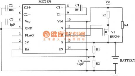
Constant-current charging circuit composed of the MIC5158 is as shown. In the whole process of charging, the circuit provides a constant current (35 mV/R3), until the battery voltage is charged to Vfl:. Vfl is float charge voltage (V). When float voltage is satisfied, MOSFET tube was turned off, and the R4 provides access forthe charge current. (View)
View full Circuit Diagram | Comments | Reading(1492)
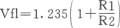
Insulation drive circuit with pulse transformer
Published:2011/9/14 6:00:00 Author:Sophia | Keyword: Insulation drive circuit, pulse transformer
Figure 1 shows that in the half-bridge and full bridge circuit of power MOSFET, how the high-pressure side switch changes to a key point.
Generally, to drive the high-pressure side of the component, a source is required between the gate pole and electrodeinsulation. If it is low-speed switch, as shown in Figure 2 dedicated driver IC constituted by the optical coupler can be used, the source terminal of the high-pressure side will make high-frequency voltage source overlap, and noise is very weak.
Therefore, In reality there are many insulation ways useing the pulse transformer insulation, but to use the pulse transformer,we need to make effor to make the circuit. (View)
View full Circuit Diagram | Comments | Reading(1340)
The simplest phase shift circuit
Published:2011/9/14 6:01:00 Author:Sophia | Keyword: simplest phase shift circuit
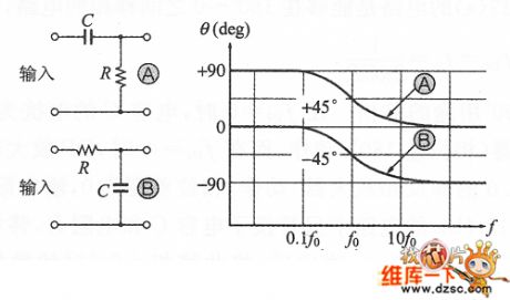
In a similar active filter circuit, usually the circuit contains the control phase circuit. This is an experiment only to change the phase of the sine wave phase-shift circuit (phase shifter) .
Following diagram shows the phase characteristics of the high-pass filter③ and low pass filter③. ③ high-pass filter can make phase shift between +90 ° ~ 0 °, while the low-pass filter ⑧ only makes phase shift between 0 ° ~ -90 °. here though phase shift is available, there is a weak point that output amplitude will change with the input frequency.
(View)
View full Circuit Diagram | Comments | Reading(1397)
Double-edge detection circuit
Published:2011/9/14 6:02:00 Author:Sophia | Keyword: Double-edge detection
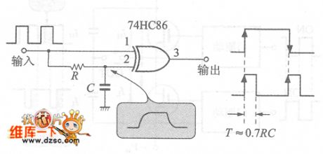
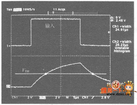
Figure 1 is the bilateral(rising and falling)detection circuit composed of XOR gate. XOR gate outputs H level when gate input terminal logic is inconsistent, for example, RC circuit easily produces delay time, the edge is detected during rising and falling, then differential pulse is outputed.
Figure 2 is the terminal voltage waveform of capacitor C. 74HC86 threshold voltage VTH is VDD / 2, the tag line is released here. From the begining of the corresponding input rising to the time to achieve the C terminal voltage VTH input, the output pulse can be obtained during the time to achieve the C terminal voltage yTH. (View)
View full Circuit Diagram | Comments | Reading(5079)
Switch delay circuit with only the delaying of rise part
Published:2011/9/14 6:03:00 Author:Sophia | Keyword: Switch delay circuit, the delaying of rise part
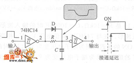
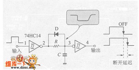
Figure 1 is the delay circuit only when the switch is ON, which is called on-delay circuit. The resistance R is in parallel with diode D, if the direction of the diode is changed, shown in Figure 2, the circuit becomes only the OFF delay time circuit- - Disconnect the delay circuit.
Figure 1 is the on-delay circuit with the delay of only rise part
Figure 2 is the off delay circuit with the delay of only the drop part The diode in the switching delay circuit reaches the action of charge and discharge time. When the diode is not conducting, T = RC; when it is conducted, CMOSIC output impedance and diode D action impedance can be neglected, which can extremely shorten time constant. (View)
View full Circuit Diagram | Comments | Reading(1188)
Switching power supply circuit with PM4020A module
Published:2011/9/14 6:01:00 Author:Sophia | Keyword: Switching power supply,
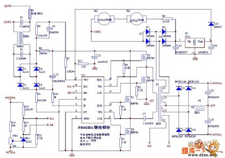
The following drawing uses switching power supply circuit with PM4020A module.PM4020A drive modules is shown by the photos, which can be used to do 200W-1500W switching power supply. PM4060A side can do 1000W-5000W switching power supply. Here is a switching power supply for sound. (View)
View full Circuit Diagram | Comments | Reading(4957)
Regulator DC-DC Circuit and Pin of Power Supply Monitor and its Main Features-MAX743 Regulator
Published:2011/9/13 23:42:00 Author:Zoey | Keyword: Regulator, DC-DC Converter, Pin, Binary Loop,
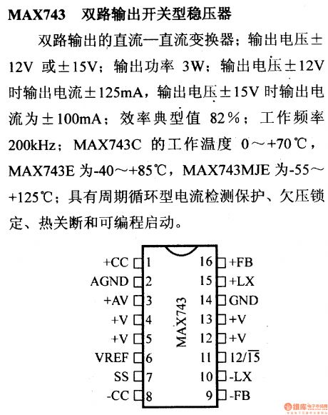
MAX743 binary loop switched regulator refers to the DC-DC converter. Its output voltage is ±12V or ±15V, and relevant output current are ±125mA ,±100mA respectively. Its output power is 3W, typical value of efficiency 82%, working frequency 200 kHz. Working temperature range of MAX743C is 0~+70℃,MAX743E -40~+85℃,MAX743MJE -55~+125℃. The regulator has a periodic circulating current detector, an undervoltage lock, a heater switch and a programmable start.
(View)
View full Circuit Diagram | Comments | Reading(930)
Regulator DC-DC Circuit and Pin of Power Supply Monitor and its Main Features-MAX742 Regulator
Published:2011/9/13 23:43:00 Author:Zoey | Keyword: Regulator, DC-DC Circuit, Pin
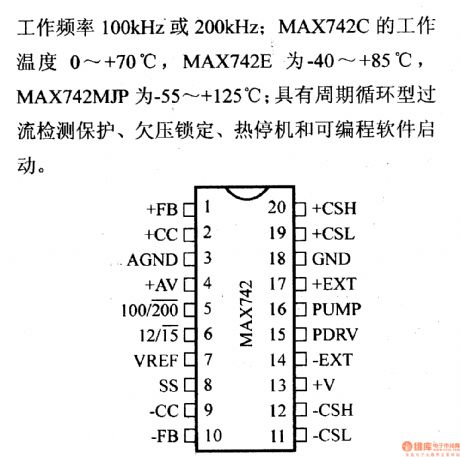
MAX742 binary loop output switched regulator refers to the DC-DC converter. Its output voltage is ±12V or ±15V, output power 3~60W, load current ±2A, output voltage range 4.2~10V, typical value of efficiency 90%.Working frequency 100kHz or 200kHz, working temperature range of MAX742C is 0~+70℃,MAX742MJP is -55~+125℃. The regulator has a periodic circulating current detector, an undervoltage lock, a heater switch and a programmable start.
(View)
View full Circuit Diagram | Comments | Reading(842)
Regulator DC-DC Circuit and Pin of Power Supply Monitor and its Main Features-MAX640/MAX653
Published:2011/9/13 23:45:00 Author:Zoey | Keyword: Regulator, DC-DC converter, Power Supply Monitor
Input voltage range of MAX640/MAX653 DC-DC converter is 4V~11.5V. Output voltage of MAX639 is 5.0V, MAX640 is 3.3V and MAX653 is 3.0V. For the converter, output current can reach 225mA, static working current is 10µA.
(View)
View full Circuit Diagram | Comments | Reading(733)
Regulator DC-DC Circuit and Pin of Power Supply Monitor and its Main Features-MAX1743
Published:2011/9/13 23:45:00 Author:Zoey | Keyword: Regulator, DC-DC Circuit, Pin of Power Supply Monitor, Converter
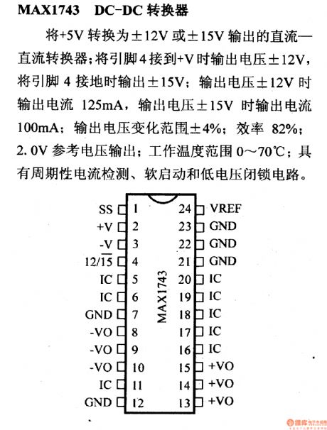
MAX1743 DC-DC converter can convert the voltage from +5V to±12V or to±15V. Connecting pin 4 to +V, andif the output current is 125mA, this converter will output ±12-V voltage; and connecting Pin 4 to the ground, the voltage output will be ±15V, and output current will be 100mA. Its output voltage range is±4%, efficiency 82%, reference voltage output 2.0V, working temperature range 0~70℃. This converter has circuits for periodic current detection, soft-start and low-voltage lock. (View)
View full Circuit Diagram | Comments | Reading(978)
Regulator DC-DC Circuit and Pin of Power Supply Monitor and its Main Features-MAX830/MAX833 DC-DC Regulator
Published:2011/9/14 0:17:00 Author:Zoey | Keyword: Regulator, DC-DC Circuit, Bipolar, PWM
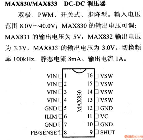
MAX830/MAX833 refers to the bipolar, PWM, switched and step-down DC-DC regulator . Its input voltage ranges from 8.0V to 40.0V. Output voltage of MAX832 is adjustable. Output voltage of MAX831 is 3.3V, MAX833 3.0V. The switched frequency of MAX830/MAX833 is 100 kHz. Static current of MAX830/MAX833 is 8mA and output current of MAX830/MAX833 is 1A.
(View)
View full Circuit Diagram | Comments | Reading(814)
Regulator DC-DC Circuit and Pin of Power Supply Monitor and its Main Features-TA78DS05P Regulator
Published:2011/9/13 23:56:00 Author:Zoey | Keyword: Regulator, DC-DC Circuit, Three-terminal Regulators

The TA78DS05P and TA78DS10P three-terminal regulators can output fixed low-margin voltage, the maximum current output is 30mA, and in a spare state, the typical voltage will be 500μA. The minimum output voltage margin is below 0.3V, and the maximum input voltage is 29V and the power is 800mW. The working temperature varies from -40 to +85℃.This circuit itself has interior overcurrent, overtemperature and short circuit- proof devices, as soon as the voltage exceeds 60V, the power supply will be cut off.
(View)
View full Circuit Diagram | Comments | Reading(751)
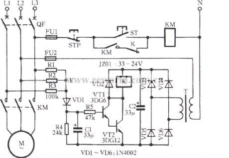
Single-phase motor main auto-winding voltage reducing and speed regulating circuit
Published:2011/9/14 20:36:00 Author:nelly | Keyword: Single-phase, motor, auto-winding, voltage reducing, speed regulating
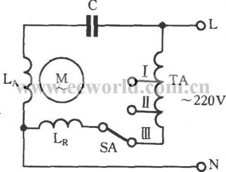
As shown in the picture, the voltage reducing characteristic of the autotransformer can be used to reduce the voltage of main winding LR directly, so that the intention of voltage reduction and speed regulation can be implemented. TA is the autotransformer; I, II, III are the gears. Because the III reduces most of the voltage, the rotation rate will be lowest when the SA reaches III. LA is the assisted winding, and LR is the main winding.
(View)
View full Circuit Diagram | Comments | Reading(1210)
One-wire remote control pump circuit
Published:2011/9/14 20:36:00 Author:nelly | Keyword: One-wire, remote control, pump
View full Circuit Diagram | Comments | Reading(811)
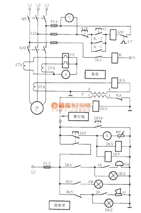
Electric relay open phase protection circuit
Published:2011/9/14 20:36:00 Author:nelly | Keyword: Electric relay, open phase, protection
Asshowninthepicture,whenthemotorisrunningnormally,thevoltageofthemiddlepoint”E”isnothighinthethree-phaseYconnectionbalancedcircuit,sotheVD1isnotConducted,andthemultiunittubes(VT1、VT22)arecutoff.TherelayKisinthestateofrelease;afterthefaulthashappened,thepoint“E”increasestowardsthezerolinevoltage.TherectificationoftheVD1makestheemitterofmultiunittubeconduct,Kactuate.Theconstantclosepointopens,andthecontactorKMloseselectricpower.MotorMstopsturningaround. (View)
View full Circuit Diagram | Comments | Reading(1685)
Doppler effect and illumination double-control automatic gate socket outlet circuit RD627
Published:2011/9/14 20:35:00 Author:nelly | Keyword: Doppler effect, illumination, double-control, automatic gate, socket outlet
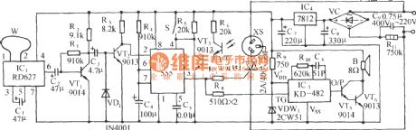
Asshowninthepicture,itiscomposedofDopplereffectsensinghead,lightcontrolswitch,monostabletrigger,SCRcontrolcircuit,musicsoundercircuit,ACvoltagereductionrectifiercircuitandsoon.Whenvehiclesandpeoplearenearthegate,thedoorwillopenautomatically;meanwhile,amelodiousmusicwillbeplayed. (View)
View full Circuit Diagram | Comments | Reading(1365)
Single bond touch sensing key design circuit
Published:2011/9/14 20:35:00 Author:nelly | Keyword: single bond, touch, ensing key, design
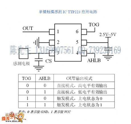
SinglebondtouchsensingchipTTP223canbeappliedfordifferentkindsofeletronic devices. The design issimple,andtheapplicationsareflexible.Thereferencecircuitisintheattachment.
Characterdescription: 2.5V~5Vwideworkingvoltagerange,3uA~5uAsuper-lowworkingcurrent SOT23-6package,smallvolume,convenientdesign ThereisonlyaCScapacityinPeripheralequipment.Thecircuitissimple Thesensingdistanceisover5cm,whichcanbeadjustedbychangingtheCScapacityparameter Variouskindsofoutputmethodscanbechosen ItcanpartlyreplacetheQT100,andthecostislow Ithasthepowerfulanti-jammingperformance,anditwillnotbetriggeredwrongly. (View)
View full Circuit Diagram | Comments | Reading(1633)
Regulator DC-DC Circuit and Pin of Power Supply Monitor and its Main Features-MAX1649/MAX1651
Published:2011/9/13 23:47:00 Author:Zoey | Keyword: Regulator, DC-DC Circuit, High-efficiency, DC-DC Controller
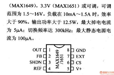
The maximum input voltage of MAX1649/MAX1651 high-efficiency DC-DC controller is 16V, output voltage of MAX1649 is 5.0V,while output voltage of MAX1651 is 3.3V. And their output voltage can also be adjusted from 1.5V to16V. If the load is between 10mA to 1.5A, efficiency will exceed 90%. Output power is over 12.5W. The maximum power-off current is 5µA, switched frequency can reach 300kHz, maximum static current of the power supply is 80µA. (View)
View full Circuit Diagram | Comments | Reading(806)
| Pages:480/2234 At 20461462463464465466467468469470471472473474475476477478479480Under 20 |
Circuit Categories
power supply circuit
Amplifier Circuit
Basic Circuit
LED and Light Circuit
Sensor Circuit
Signal Processing
Electrical Equipment Circuit
Control Circuit
Remote Control Circuit
A/D-D/A Converter Circuit
Audio Circuit
Measuring and Test Circuit
Communication Circuit
Computer-Related Circuit
555 Circuit
Automotive Circuit
Repairing Circuit