
Circuit Diagram
Index 873
OP_AMP_DC_COUPLING_AND_OFFSET
Published:2009/7/20 3:14:00 Author:Jessie
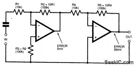
Dc interstage coupling might be tolerable in terms of offset errors (View)
View full Circuit Diagram | Comments | Reading(657)
1_watt_OTL_audio_power_amplifier_using_an_ECG1035
Published:2009/7/20 3:13:00 Author:Jessie
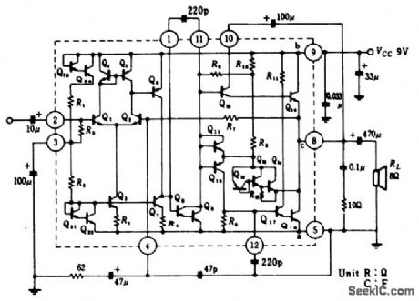
1-watt OTL audio power amplifier using an ECG1035. Packaging on the ECG1035 is a 12-pin plastic flat pack with metal tabs. Recommended supply voltage is 9 volts. Voltage gain is 50 dB. Frequency response is from 50 hertz to 100 kilohertz (courtesy GTE Sylvania Incorporated). (View)
View full Circuit Diagram | Comments | Reading(807)
OP_AMP_DC_FEEDBACK_STABILIZATION
Published:2009/7/20 3:13:00 Author:Jessie
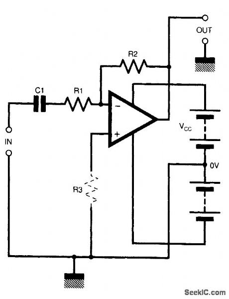
Blocking capacitor C1 ensures that dc negative feedback is maximized. (View)
View full Circuit Diagram | Comments | Reading(641)
55_watt_OTL_audio_power_amplifier_using_an_ECG1037
Published:2009/7/20 3:12:00 Author:Jessie
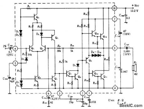
5.5-watt OTL audio power amplifier using an ECG1037. Typical voltage gain is 55dB. Frequency response is from 30 hertz and 50 kilohertz. Input impedance is 36K (courtesy GTE Sylvania Incorporated). (View)
View full Circuit Diagram | Comments | Reading(689)
VSUBCC_SUB__AUDIO_NOISE_REDUCER
Published:2009/7/20 3:12:00 Author:Jessie
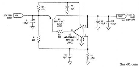
The circuit reduces noise and ripple voltage by 40 dB over the 100-Hz to 20-kHz audio range. It provides a clean source of 5-V power for driving audio circuits in portable applications such as cellular phones and multimedia notebook computers. Most linear regulators reject noise only up to 1000 Hz or so, and the bulk of a low-frequency passive filter is unwelcome in portable applications. The circuit shown accepts noisy Vcc in the 4.5- to 6-V range and produces quiet Vcc at a dc level 7 percent lower. For example, it produces 4.65 V at 1 A from a nominal 5-V source, with only 200 μA of quiescent current. The largest capacitor is 10 μF and the resistors can be 0.1 W or surface-mount 0805 size. When operating, the circuit acts as a wide-bandwidth buffered voltage follower (not a regulator) whose dc output level is 7 percent below Vin。 R1 and R3 form a voltage divider that provides the 7 percent attenuation, and C4 helps to form a 93-percent filter replica of Vin at the op amp's inverting input. The op amp's small input bias current (25 nA typical) allows large resistor values for R1 and R3, yet limits the maximum dc error to only 20 mV. The result is a low-pass filter with a 2-Hz corner frequency that provides 20 dB of attenuation at 20 Hz. (View)
View full Circuit Diagram | Comments | Reading(1254)
OVERLOAD_PROTECTION_FOR_SERIES_REGULATOR
Published:2009/7/20 3:12:00 Author:Jessie
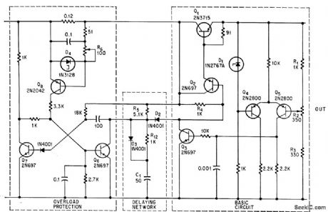
For input voltage of 30 to 40 v d-c, output at full load of 3 amp will be held within 99.09% of 28 v. Tunnel diode D4 and transistor Q8 in overload-sensing circuit trigger monostable mvbr Q6-Q7 to remove drive from Q1 until mvbr resets.-J.Takesuye, Tunnel-Diode Sensor Protects Regulator from Short Circuit, Electronics, 38:25, p 75-76. (View)
View full Circuit Diagram | Comments | Reading(886)
TUBE_ZENER_REGULATOR
Published:2009/7/20 3:10:00 Author:Jessie
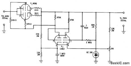
Regulates within 0.2 v from no load lo full load. Variation of 10% in line voltage causes only 0.1 v output change.- Zener Diode Handbook, Intenational Rectifier Corp., 1960, p 59. (View)
View full Circuit Diagram | Comments | Reading(903)
LARGE_VOLTAGE_SWING_WITH_WIMITED_SUPPLY_VOLTAGES
Published:2009/7/20 3:08:00 Author:Jessie
Circuit shows usual solution to problem, wherein final transistor is operated near positive supply voltage and zener diode provides coupling. Drop in gain caused by R can be eliminated by using constant-current diode in place of R. If R1, R2, and R3 are similarly replaced with these diodes, circuit becomes independent of positive line, eliminating spurious feedback through this line.-T. K. Hemingway, Applications of the Constant-Current Diode, Electronics, 34:42, p 60-63. (View)
View full Circuit Diagram | Comments | Reading(878)
CONTROL_FUNCTION_DECODER
Published:2009/7/20 3:07:00 Author:Jessie
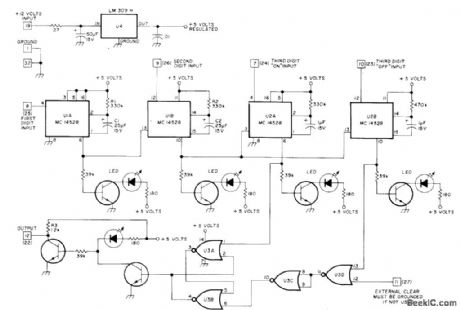
Circuit detects predetermined 3-digit sequence of Touch-Tone signals and sets flip-flop to provide required output for activating desired function.Another 3-digit sequence, differing in only third digit, resets flip-flop for turning off controlled device. Circuit uses two dual mono MVBRs. Output of U1A goes to reset terminal of U1B.Output of U1B goes to reset terminals of monos U2A and U2B. Mono outputs drive RS flip-flop to provide output required for desired control fu notion, such as control of autopath, switching repeater mode from carrier to tone-access, and switching to remote receiver. Q1-Q6 can be almost any NPN silicon transistors, such as 2N3904. U3 can be MC14001 or CD4001. Numbers in boxes and parentheses refer to edge connector pins.-T. E. Doyle, Control Function Decoder, Ham Radio, March 1977, p 66-67. (View)
View full Circuit Diagram | Comments | Reading(992)
FM_detector_stage_using_one_ECG708_IC
Published:2009/7/20 3:06:00 Author:Jessie
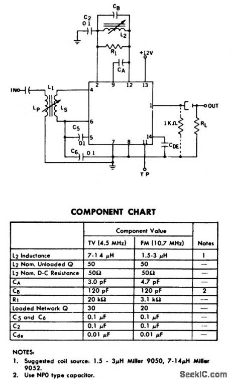
FM detector stage using one ECG708 IC. The output can be employed to directly drive a transistor power output stage. Either a 4.5 MHz IF or a 10.7 MHz IF can be detected(see component chart). An output of 0.6 volt can be obtained with less than 1% distortion. The output of the three-stage amplifier at the input is brought out to pin 10 so that the chip can be used as a wide-band 60 dB amplifier (courtesy GTE Sylvania Incorporated). (View)
View full Circuit Diagram | Comments | Reading(710)
50_CPS_2_KG_REGULATOR
Published:2009/7/20 3:06:00 Author:Jessie
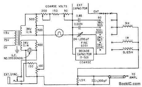
Thermal bridge using ordinary iron-wire ballast tube is used with tunable filler of 200 via variable-frequency power supply for instrument calibration. Output stage (not shown) uses two 7378 pentodes in push-pull class AB1, with positive feedback.-E. A. Gilbert, Precision Variable Frequency Power Supply, Electronics, 34:2, p 99-100. (View)
View full Circuit Diagram | Comments | Reading(700)
DELAYED_VOX
Published:2009/7/20 3:06:00 Author:Jessie
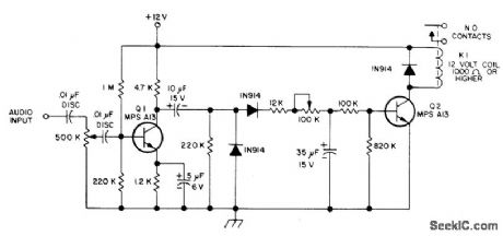
Minimizes unintentional triggering of repeater by using timer requiring 3 s of continuous carrier and audio on input receiver of repeater to turn on transmitter. Repeater is then controlled by its own carrier-operated relay until 20-s lapse in transmission occurs. System then requires another3-s carrier to restore normal operation, Q1 is common-emitter amplifier with gain adjusted by 500K pot. Audio peaks from al feed full-wave diode detector through 10-ptF electrolytic. Series resistance in path through 35-ptF electrolytic controls its charge-up time and thus controls delay of relay pickup. Adjust 100K pot to give desired turn-on delay in range from fraction of second to about 4 s. Resistance divider shown provides relay dropout delay of about 20 s, which pre-vents VOX circuit from dropping out repeater during lapses in speech.-J. Everhart, A Delayed VOX for Repeaters, 73 Magazine, April 1974, p 17 and 19-20. (View)
View full Circuit Diagram | Comments | Reading(5604)
FM_stereo_demodulator_with_indicator_lamp_using_an_ECG1106_16_pin_DIP
Published:2009/7/20 3:05:00 Author:Jessie
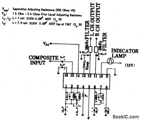
FM stereo demodulator with indicator lamp using an ECG1106 16-pin DIP.Input impedance is 20K,The indicator lamp operates at a 19 kHz input level of 5 mV RMS. Audio muting on voltage is 0.75 volt and off voltage is 1.0 volt(courtesy GTE Sylvania Incorporated). (View)
View full Circuit Diagram | Comments | Reading(645)
PERIODIC_60_Hz_NOISE_ELIMINATOR
Published:2009/7/20 3:05:00 Author:Jessie
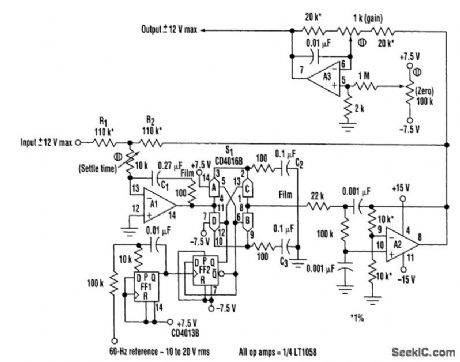


This analog/digital synchronous-averager circuit implements a robust comb filter that (theoretically) infinitely attenuates all 60-Hz harmonics. It does this independently of precision component tolerances. Signal components with frequencies below 20 Hz are passed virtually undisturbed. In the circuit, A1 continuously integrates and inverts the sum of the input signal and the output of buffer amplifier A2. Depending on the state of FF2, either switches S1A and S1B or S1C and S1D will conduct. Because flip-flop FF2 toggles once each 60-Hz cycle, A1 always integrates the difference between the instantaneous input voltage and the integral of the input taken over the preceding cycle. The transfer function of such a piecewise integration is characterized by a series of impulses that occurs atƒ (the fundamental frequency of the integration cycle) and at all integer multiples ofƒ This extreme attenuation of harmonic noise is not limited by component tolerance. The filter's setting time for an input step, however, does depend upon the trimming of potentiometer P1. Optional unity-gain inverter A3 undoes the signal inversion performed by A1 and incorporates trimmer pots P2 and P3 for precise adjustment of overall filter gain and zero offset. (View)
View full Circuit Diagram | Comments | Reading(1729)
107_MHz_FM_IF_amplifier_with_detector
Published:2009/7/20 3:04:00 Author:Jessie
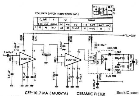
10.7 MHz FM IF amplifier with detector.coil data for the transformer is shown in the table,The ECG1100 is a 7-pin module,Typical voltage gain per unit is 56 dB,Total supply current for the entire circuit is 21 mA.The detector output for a 60 dB Input is go mV(courtesy GTE Sylvania Incorporated). (View)
View full Circuit Diagram | Comments | Reading(3880)
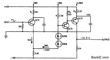
BACKWARD_WAVE_OSCILLATOR_FILAMENT_SUPPLY
Published:2009/7/20 3:04:00 Author:Jessie

Provides constant voltage for filament of backward-wave oscillator. Output voltage is compared with fixed reference in d-c amplifier, and difference is used to control series pass element.-S. Prigozy, Designing Special Power Supplies for Voltage Tunable Oscillators, Electronics, 35:44, p 48-50. (View)
View full Circuit Diagram | Comments | Reading(810)
TONE_BURST_FOR_MIKE
Published:2009/7/20 3:04:00 Author:Jessie
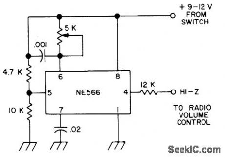
Uses NE566 PLL function generator to provide tone entry into 2-meter repeaters. Output is fed into volume control of any AM transistor radio, and loudspeaker is held in front of transceiver microphone when tone is desired.-F. J. Derfler, An Acoustically Coupled Digital Keyed Squeaker for Tone Burst Entry, 73Magazine, Aug, 1973, p 27-30. (View)
View full Circuit Diagram | Comments | Reading(823)
CROWBAR
Published:2009/7/20 3:03:00 Author:Jessie
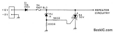
Developed to protect portable repeaters from reverse or excessive voltage when operating on emergency power supply. Zener voltage rating determines maximum voltage that can reach repeater. Diode prevents damage by incorrect polarity. Use fast-blowing fuse.-Circuits, 73Magazine, April 1977, p 164. (View)
View full Circuit Diagram | Comments | Reading(2845)
AM_FM_F_amplifier_with_AF_amplifier
Published:2009/7/20 3:03:00 Author:Jessie
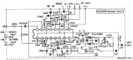
AM/FM F amplifier with AF amplifier.Note in the diagram that the AF amplifier is not connected to the detector output.To use the AF amplifier connect the detector output to the AF input.The AF output with 1 kHz at 1 mV input is 0.47 volt typically(courtesy GTE Sylvania Incorporated). (View)
View full Circuit Diagram | Comments | Reading(680)
12_V_REGULATED_SUPPLY_WITH_REFERENCE_AMPLIFIER
Published:2009/7/20 3:03:00 Author:Jessie
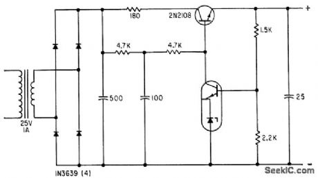
Integrated transistor and zener diode in reference amplifier act with tansistor 2N2108 lo hold 12.v d-c output voltage within 0.3% over ac line voltage variations of 10% for load currents up to 100 ma-T. P. Sylvan, New Device Simplifies Power Supply Design, Electronics, 36:20, p 39-43. (View)
View full Circuit Diagram | Comments | Reading(705)
| Pages:873/2234 At 20861862863864865866867868869870871872873874875876877878879880Under 20 |
Circuit Categories
power supply circuit
Amplifier Circuit
Basic Circuit
LED and Light Circuit
Sensor Circuit
Signal Processing
Electrical Equipment Circuit
Control Circuit
Remote Control Circuit
A/D-D/A Converter Circuit
Audio Circuit
Measuring and Test Circuit
Communication Circuit
Computer-Related Circuit
555 Circuit
Automotive Circuit
Repairing Circuit