
power supply circuit
Index 52
Intelligent pulse electric bicycle charger principle diagram
Published:2011/11/13 20:48:00 Author:May | Keyword: Intelligent pulse, electric bicycle, charger
Voltage driving type pulse width modulator
1. feature and function of TL494
TL494 is produced by the United States IR company. It is voltage driving type pulse width modulator, which can be used as switching power circuit in display, computer and other system circuit. The output triode of TL494 can connect to the mode of common emitter or emitter follower. So it can choose the double-end push-pull or single-end output mode. When ituses push-pull output mode, the differ of two drive pulse is 180°, but when it is single end mode, its two ways ofdrive pulse have the same frequency and same phase.
The internal function diagram of TL494 is shown in the following diagram
1IN+, 1IN-, 2IN+, 1IN input; FEEDBACK feed-back; DTC non load control; CT timing capacitor; RT timing resistor; GND ground; C1, C2 collector 1, 2; E1, E2 emitter 1, 2; Vcc power supply; OUTPUT CTR output control; REF reference.
2, application circuit
(View)
View full Circuit Diagram | Comments | Reading(3724)
Electric bicycle intelligent charger using UC3845
Published:2011/11/10 2:55:00 Author:May | Keyword: Electric bicycle, intelligent charger
UC3845 is high-performance, single-end output current-mode PWM control circuit. Its biggest advantagesare fewer external components without independent auxiliary power supply, and simple external circuit assembly and low cost. Electric fly-back controllingbike uses it assmart charger, whichis very competitive in the market. The whole circuit principle is shown in Figure 1. Figure 2 is an internal block diagram of UC3845. Each pin function of UC3845 is shown in Table 1. The novelty of the circuit is that it does not use internal error amplifier IC1 (reasonably, pin 2 is the namely reversed end and itshould be grounded), but it directly uses second precision voltage regulator IC3 AS431for adjusting and controlling. In the following diagram, we will try to interview it. (View)
View full Circuit Diagram | Comments | Reading(11103)
Emergency light using 6V battery cell automatic charger circuit 2
Published:2011/11/13 20:40:00 Author:May | Keyword: Emergency light, 6V, battery cell, automatic, charger
If it works forlong hours, its fever is serious, and it is easily to be destroyed. It is easily tolead to over-charge to cause the prematurely dry of electrolyte and shorting the battery life. For the shortcomings, the author changes it to auto-charger. After using six months, it works well. The circuit is shown in the above diagram.
Principle outline
It offers reference voltage for the base of T1. Relay J can achieve self-locking and automatic power off. When it is connected to the battery, K is pressed, power indicator L is lit, meanwhile J is energized and pulled in, K is self-locked by its contact J-0, and charging is starting. At this time, battery cell is under electrical, so T1 emitter voltage is less than (7.5V +0.65 V), T1 is cut off, T2 is also cut off, and this has no effect on the T3. When the battery voltage is charged to 7.5V, Tl emitter voltage is 7.5V +0.65 V, T1 is saturated and broken over, T2 is also broken over, T3 is cut off because its base voltage is dropped down, J is lost power and release, J-0 is cut, charging is stopped. Indicator light L goes out. It can charge to different voltage battery by adjusting W. (View)
View full Circuit Diagram | Comments | Reading(2533)
4A/12.3V lithium ion battery charger circuit with LTC4008 control chip
Published:2011/11/24 1:01:00 Author:May | Keyword: 4A/12.3V , lithium ion , battery charger, control chip
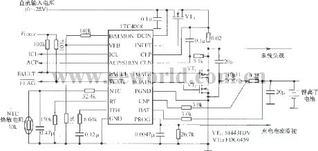
4A/12.3V lithium ion battery charger circuit uses LTC4008 as control chip.
(View)
View full Circuit Diagram | Comments | Reading(1746)
Storage battery automatic charger 3
Published:2011/11/10 2:44:00 Author:May | Keyword: Storage battery, automatic charger

Familiar storage battery automatic charger can achieve the purpose of automatic control by detecting storage battery voltage when it ischarging. But when it has charging current, justified voltage of storage battery will be too high, so it is hard to decide the degree of charging by storage battery voltage. This text introduces an automatic storage battery charger.
The circuit is shown in diagram 4-10. It is theautomatic charger and its core is thethyristor components. When charger is connectedto discharged storage battery, thyristor VS is breaking over at every positive half period, and it will charge to the battery. In the end of positive half period, when charge voltage is lower than storage battery voltage, thyristor VS is cut off. When positive half period sarts, VS is in the cut-off stateat this time, the comparing of charge voltage and reference starts in order to decide whether VS is breaking over or not. When justified voltage of battery reaches to the certain value (about 13.5V), VT will not have current and VS will be cut off. (View)
View full Circuit Diagram | Comments | Reading(1517)
Two way constant pressure source using two operational amplifier
Published:2011/11/23 1:12:00 Author:May | Keyword: Constant pressure source, operational amplifier
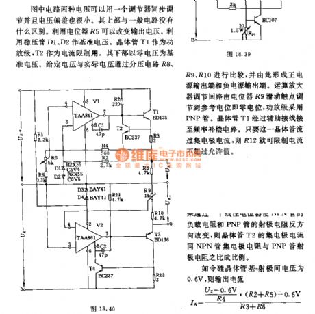
Thetwo kinds of voltageof the circuit in the diagram can use a adjustor to dosynchronization regulation and the voltage deviation is very small. Its upside has no difference with normal circuit. The potentiometer R5 can change theoutput voltage.The voltage regulator tubes D1, D2 can be used as reference voltage. Transistor T1 is used as amplifier class, T2 is usedfor current limiting. Its downside uses zero voltage as voltage reference. Given voltage and virtual voltage compares through divider circuit R8, R9, R10 to generate opsitive power supply output end and negative power supply output end. Operational amplifier regulating loop uses regulation resistor R9 sliding contact to adjust to reference potential, namely zero potential, amplifier class uses PNP transistor. (View)
View full Circuit Diagram | Comments | Reading(1014)
New type nickel-cadmium battery and battery charger
Published:2011/11/10 2:41:00 Author:May | Keyword: New type, nickel-cadmium battery, battery charger
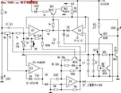
The principle of this circuit is shown in the following diagram. IC1, IC2, IC3 make up voltage comparator. IC4 is square wave pulse generator. The pulse width and frequencyare controlled by IC1. When IC4 outputs positive pulse, BG4 is turned on, constant current IC3 is charging to battery. When IC4 outputs negative pulse, the output is differentiationed by C2. Then itmakes BG1 and BG2 turn on in a short time. It is discharged to battery.
IC1's output is inhigh level afterthepower turningon. The circuit willbe incharging state. If itneeds to discharge, we should touch discharging button AN. It can make IC1 output low level. BG1, BG2are turned on. The battery starts to discharge. Discharge light LED3 is bright. Charging light LED3 is extinguished. When battery discharges to 0.9V, IC1 outputs high level. BG1, BG2are cut off. Discharging is finished. Charging starts.
When battery is charging to 1.42V, IC1's output is changed low level from high, IC2's output is changed high level from low. (View)
View full Circuit Diagram | Comments | Reading(1284)
Voltage limiting nickel-cadmium battery charger circuit
Published:2011/11/10 2:37:00 Author:May | Keyword: Voltage limiting , nickel-cadmium battery charger
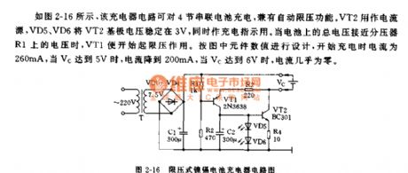
As shown in diagram 2-16, this charger circuit can charge to four series battery. This circuit also has theautomatic voltage limiting function. VT2 is used for current source. VD5, VD6 and VT2 can stabilize VT2's base voltage at 3V. Meanwhile they are used as charge lights. When the total voltage on the battery closes to the voltage on voltage divider R1, VT1 will start thevoltage limiting function. It is designed according to numeral value of element in the diagram, the currentis 260mAwhen it starts to charge, when Vc reaches to 5V, the current drops to 200mA, when Vc reaches to 6V, the current is almost zero. (View)
View full Circuit Diagram | Comments | Reading(1505)
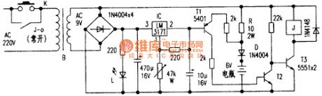
Nokia 8210 mobile phone travel charger circuit
Published:2011/11/13 20:34:00 Author:May | Keyword: Nokia, mobile phone, travel charger
Nokia 8210 mobile phone travel charger is produced in shanghai, Its crust has label: input AC220V/50Hz (≤30mA), output 4.2V (≤200mA). When it is used in charging, when itneed thecharging Li battery with label 3.6V chaging at 3.98V, the red lamp in the charger circuit is gone out, the green lamp is lit. The whole charging time is about four hours. The author dissects this charger, and draws the circuit diagram. It is referenced by readers when they use or preserve it. Operational amplifier IC in the circuit is used as compartor.
(View)
View full Circuit Diagram | Comments | Reading(2735)
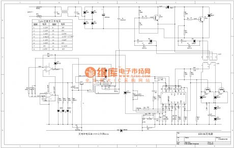
Nickel-cadmium battery with 6v (12v) / 2A automatic charging device
Published:2011/11/13 20:31:00 Author:May | Keyword: Nickel-cadmium battery, 6v (12v) / 2A, automatic, charging device
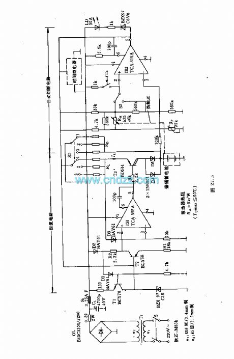
This automatic charging device can make sure that battery has best charging processto prevent over load. It has three charging modes in application: stand charging, continue (mini-flow) charging and fast charging. They have some differences in charging current and cut-off charging process. The device includes two parts: constant current circuit and automatic cut-off circuit. The table shows resistor RL and RD value when thereis difference in charging current.
(View)
View full Circuit Diagram | Comments | Reading(1242)
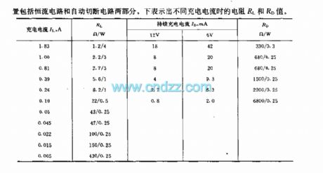
Programmable automatic charger circuit
Published:2011/11/10 2:30:00 Author:May | Keyword: Programmable, automatic charger
Working principle
The circuit diagram is shown in diagram 4-26. The electric supply is bucked by transformer, rectified bydiode, filtered bycapacitor to output 18V pulse voltage, then it outputs 12V steady voltage through three terminal regulator W7812 after it outputs 18V pulse voltage. VD1 is used for working indication. Decade counter CD4017 etc makesup thecharging, discharging driver circuit. CP end is added 50Hz AC signal. Output ends Q0~Q9 appear high level one by one. V1 etc makes up charge executive switch; V2 makes up the discharge execute switch; V3, V4, VD9 etc make up battery charger indicator and power-off executive switch. When CD4017's output ends Q1~Q5 output high level, V1 is turned on, and the circuit starts to charge to battery pack. When Q6 outputs high level, V2 is turned on, battery pack starts to discharge. When Q9 outputs high level, V3, V4 start to detect the charge voltage. When battery pack is full charged, V3 is turned on, LED VD9 is lit. It indicates that battery is full charging. Meanwhile V4 is turned on. CD4017's pulse input end will be forbidden, Q9 will keep high level and do not change. It offers trickle charge only by R7. If battery is not full charged, V3, V4are failure to actuate, CD4017 will work on. (View)
View full Circuit Diagram | Comments | Reading(1585)
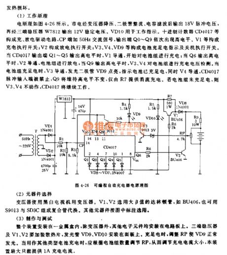
Simple and fully automatic charger circuit
Published:2011/11/13 20:10:00 Author:May | Keyword: Simple, fully automatic, charger
As shown in diagram 4-1, voltage regulator tube VD2 is cut off when the voltage of charged storage battery is lower than desired value. Voltage regulator tube VD2 is turning on only when the voltage on storage battery reaches to desired value. Triode VT can be turned on by adjusting resistor RP. Relay K1 is pulled in, thereby K1-1, K1-2are cut off. At this time LED1 (green) is turning off, LED2 (red) is lit (LED1, LED2are lit when it is starting up) to indicate chargebeing end. Needed voltage value depends on the value of voltage regulator tube. Electrolytic capacitor C is used for filtering pulse current voltage on relay after half wave rectifying. If you do not use C, relay may generate continuous action. Relay can not generate continuous action by adjusting RP. R2 is current limiting resistor of VD2. It can not too big or too small. (View)
View full Circuit Diagram | Comments | Reading(1286)
Switch voltage regulator circuit using 110V voltage doubling/220V alternating voltage input
Published:2011/11/30 21:45:00 Author:May | Keyword: Switch voltage regulator, 110V voltage doubling/220V alternating voltage input
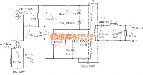
This power supply circuit is shown in the diagram, input alternating voltage is 110V or 220V. When 110V alternating voltage power supply changesin the range of 85~132V or 220V alternating voltage power supply changesin the range of 170~265V, Sv=±1%. When load current change range is 10%~100%, Si=±5%. Output ripple voltage is ±50mV. S is 110V/220V alternating voltage option switch in the circuit, and it can bereplaced by cable jumper on printed plate. When S is closed, you can choose 110V alternating voltage input, at this time, rectifier bridge BR and resistor-capacitor components and parts R1, C1, R2, C2 make up voltage doubling rectifing circuit. When S opens, you can choose 220V alternating voltage input. In order to improve stability of voltage, you can add resistor R4 in output circuit, and the least load setted by it is 36mA.
(View)
View full Circuit Diagram | Comments | Reading(3739)
Charging circuit using UBA2008 charging switch chip
Published:2011/11/30 20:28:00 Author:May | Keyword: Charging circuit , charging switch chip
UBA2008 is the charging intelligent management chip with pulse way produced by Philips. The device integrates a low- resistance power switch which can be used for charge controlling of single cell Li-Ion or three NiMH cells or in the pre- charging or fast charging modes. It has current limiting , overvoltage protection, thermal protection and electrostatic discharge (ESD) protection, and it integrates the security mechanisms in battery charging process to ensure its safe operation.
(View)
View full Circuit Diagram | Comments | Reading(1110)
Constant pressure source adopts operational amplifier TAA861
Published:2011/11/10 0:16:00 Author:May | Keyword: Constant pressure source, operational amplifier
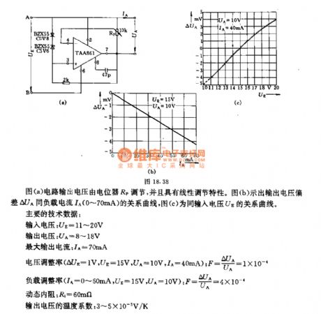
Diagram (a) circuit's output voltage is adjusted by regulation resistor Rp, and ithas regulating characteristics . Diagram (b) is the relationship curve of output voltage bias ΔUAandload current IA (0~70mA), diagram (c) is the relationship curve of input voltage UE.
Main technical data
input voltage: UE=11~20V
output voltage:UA=8~18V
maximum output current: IA=70mA
voltage regulation factor (ΔUE=1V, UE=15V, UA=10V, IA=40mA); F=ΔUA/UA=1×10-4
load regulation factor (IA=0~60mA, UE=15V, UA=10V); F=ΔUA/UA=4×10-4
dynamic resistance: Ri=60mΩ
output voltage temperature coefficient: 3~5×10⁻⁵V/K (View)
View full Circuit Diagram | Comments | Reading(1190)
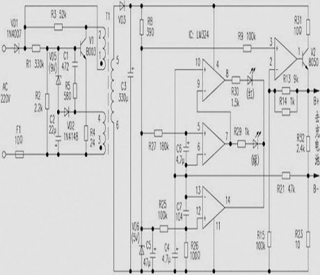
Multi-functional automatic charger circuit
Published:2011/10/26 21:17:00 Author:May | Keyword: Multi-functional automatic charger
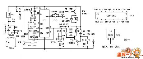
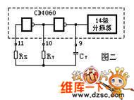
The working principle is shown in Figure one. It is the controller with CD4060 being the core. CD4060 is the 14-bit binary serial counting/frequency divider and oscillator. It has two parts: one is the 14 levels of frequency divider, and its frequency division coefficient is 16-16384 (it is output by Q4,¯Q14). Another part is the oscillator, which may be the RC oscillator composed of the external connecting resistor and capacitor. f=1/2.2RT CT. It is shown in Figure two. This installment is the oscillator composed of the C4, R2, R3, and the frequency approximately is the 0.2Hz. LED2 is the bi-color light emitter diode.
(View)
View full Circuit Diagram | Comments | Reading(2466)
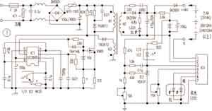
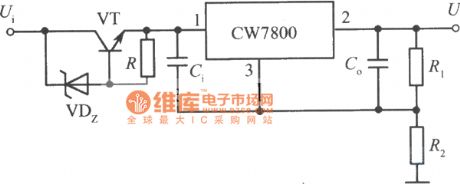
High input-high output integrated regulated power supply circuit circuit diagram 2
Published:2011/8/19 2:30:00 Author:Jessie | Keyword: High input-high output , integrated regulated power supply
View full Circuit Diagram | Comments | Reading(772)
High input-high output integrated regulated power supply circuit circuit diagram 1
Published:2011/8/19 2:30:00 Author:Jessie | Keyword: High input-high output , integrated regulated power supply

View full Circuit Diagram | Comments | Reading(815)
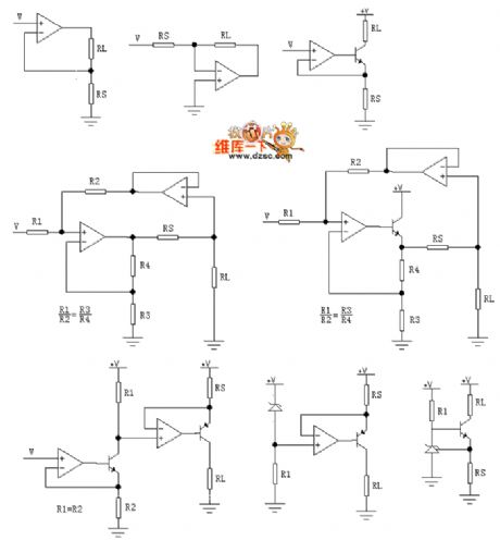
Several vi transformation and constant current source circuits
Published:2011/12/8 20:19:00 Author:Ecco | Keyword: Several vi transformation , constant current source
View full Circuit Diagram | Comments | Reading(1696)
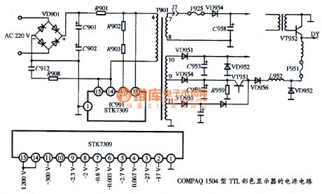
The power circuit of COMPAQ 1504 TTL color monitor
Published:2011/12/8 0:57:00 Author:Ecco | Keyword: power circuit , COMPAQ , TTL , color monitor
View full Circuit Diagram | Comments | Reading(935)
| Pages:52/291 At 204142434445464748495051525354555657585960Under 20 |
Circuit Categories
power supply circuit
Amplifier Circuit
Basic Circuit
LED and Light Circuit
Sensor Circuit
Signal Processing
Electrical Equipment Circuit
Control Circuit
Remote Control Circuit
A/D-D/A Converter Circuit
Audio Circuit
Measuring and Test Circuit
Communication Circuit
Computer-Related Circuit
555 Circuit
Automotive Circuit
Repairing Circuit