
Basic Circuit
Index 187
OP_AMP_ERROR_SOURCE_CIRCUIT
Published:2009/7/13 2:06:00 Author:May
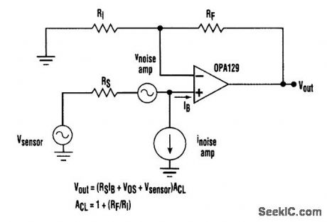
The basic error sources for an op amp are shown referenced to the output. In high-source-imbecome quite dominant. pedance applications, the input bias current terms can become quite dominant. (View)
View full Circuit Diagram | Comments | Reading(793)
OP_AMP_BIAS_PRECAUTION_CIRCUIT
Published:2009/7/13 2:05:00 Author:May
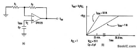
All amplifiers must have a dc path for input-bias current to return to ground (a). Without this path, an amplifier will eventually drift to the output rail (b). (View)
View full Circuit Diagram | Comments | Reading(704)
3_min_TO_4_h
Published:2009/7/13 2:02:00 Author:May
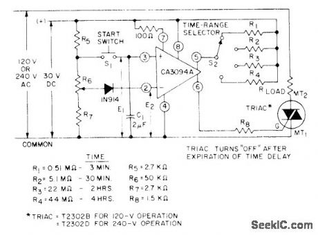
Presettable analog timer achieves long time intervals by discharging C1 into input terminal 3 of CA3094 programmable opamp, which provides sufficient output current for driving thyristors and other control devices.- Circuit ldeas for RCA Linear ICs, RCA Solid State Division, Somerville, NJ, 1977, p 8. (View)
View full Circuit Diagram | Comments | Reading(862)
5 V to 12 V booster circuit diagram
Published:2011/7/18 10:38:00 Author:Nancy | Keyword: 5 V to 12 V , booster
View full Circuit Diagram | Comments | Reading(861)
4_h_CONTROL_FOR_TRIAC
Published:2009/7/13 2:00:00 Author:May
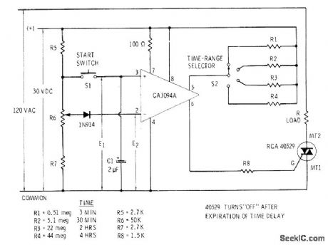
Time at which triac is triggered by IC after momentarily pressing start switch is determined by resistor values used, When switch is released, charging capacitor C1 begins its long discharge interval. When voltage E1 becomes less than E2, pin 2 draws current and serves to reverse polarity of output at pin 6 for triggering triac. Diode limits maximum differential inputvoltage.-E. M. Noll, Linear IC Principles, Experiments, and Projects, Howard W. Sams, lndianpolls, IN, 1974, p316-317. (View)
View full Circuit Diagram | Comments | Reading(933)
117_VAC_FROM_24_60_VDC
Published:2009/7/13 2:00:00 Author:May
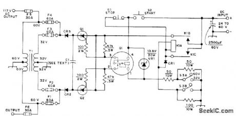
Will operate from either 24- or 32-V storage battery or from 60-VDC source. Circuit shown is set up for 60-V operation. For 24/32 V, remove F1 and F4 andinsert F2 and F3, then switch S3 to 32 V. T1 is 117-V 20-A Variac with bifilar primary winding added; use 38 bifilar turns of No. 8 for 24 V and 48 turns for 32 V. Commutating capacitor C1 consists of ten 120-μF 400-VDC oil-filled capacitors (do not use electrolytics). SCRs Q1 and Q2, rated 100 A at 800 PIY (Poly Paks 92CU1167), are switched by Cornell-Dubilier 98600 60-Hz 12-V vibrator.VR1, which limits voltage across vibrator coil, consists of two 6.8-V 10-W zeners. With 60-V operation, use 1-ohm 200-W resistor in series with inverter while starting, but short it out while inverter is running. Inverter output voltage varies from 150 VAC no-load to 110 VAC with 1650-W resistive load. CR1 is 400-PIV 200-A silicon. CR2 and CR3 are 800-PIV 250-A silicon.-R. Dunaja, A High-Power SCR Inverter,QST, June 1974, p 36-37. (View)
View full Circuit Diagram | Comments | Reading(802)
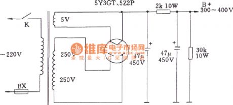
Direct heating rectifier tube full-wave rectifier and filter circuit diagram
Published:2011/8/4 1:32:00 Author:Ecco | Keyword: Direct heating, rectifier tube , full-wave rectifier , filter circuit
View full Circuit Diagram | Comments | Reading(1333)
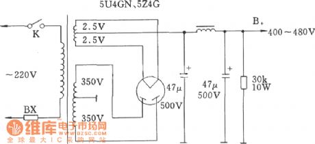
The high-voltage circuit diagram of DC rectifier tube filament center-tap
Published:2011/8/4 1:27:00 Author:Ecco | Keyword: high-voltage , DC rectifier tube , filament center-tap
View full Circuit Diagram | Comments | Reading(1193)
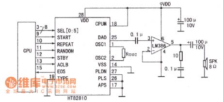
Array speech synthesis series circuit diagram
Published:2011/8/4 1:25:00 Author:Ecco | Keyword: Array speech synthesis
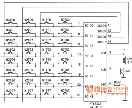
The speech synthesis circuit uses four series more input or output components to form the matrix keyboard. Figure shows HT83XXX series of 32-key application circuit diagram. This series of voice circuits can achieve statement spelling and other functions by plugging the microprocessor (CPU).
This is the connection diagrambetween the CPU and HT82810.
(View)
View full Circuit Diagram | Comments | Reading(1508)
HT16500 audio integrated chip circuit diagram
Published:2011/8/4 1:39:00 Author:Ecco | Keyword: audio integrated chip
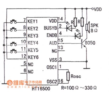
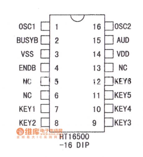
Theplastic DIP pin diagram and the typical application circuit of HT16500audio integrated circuit are as below:
(View)
View full Circuit Diagram | Comments | Reading(703)
rotary disc switch principle circuit
Published:2011/7/19 10:19:00 Author:Nancy | Keyword: rotary disc switch
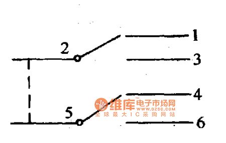
This switch looks very complex, it is actually a double pole double throw switch. The welding piece 2 and 5 are pole , and the other four leading welding pieces are throw (shown as the figure). When the rotary disc turns to + , 2 and 3 conduct, 5 and 6 conduct; When the rotary disc turns to - , 2 and 1 conduct, 5 and 4 conduct. Through the rotary disc has ten teeth, and can turn ten times, but there are only + and - two states mentioned as aobove. (View)
View full Circuit Diagram | Comments | Reading(606)
BASIC_BOOST_CONVERTER_CIRCUIT
Published:2009/7/13 1:43:00 Author:May
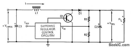
This boost converter with a single switching transistor depends on the transformer for energy storage. (View)
View full Circuit Diagram | Comments | Reading(1021)
500_kHz_33_V_TO_12_V_DC_CONVERTER
Published:2009/7/13 1:43:00 Author:May
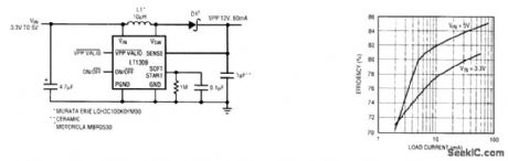
The LT1309 500-kHz micropower dc-to-dc converter circuit shown provides a compact 12-V supply. High-frequency operation permits the use of low-inductance and low-capacitance values for surface-mount parts. The LT1309 provides 60 mA of output current at 12 V, required for 8-bit-wide flash memory chips. In addition, when the flash memory card is removed, the LT1309 can be shut down by the system, reducing current draw to 6 μA. A soft-start feature allows the output voltage to ramp up to 12 V over a period of time, minimizing inrush current needed from the 3.3-V supply to charge the PCMCIA input capacitance. An active-low VPP VALID output signals the system that the 12-V supply is within regulation after being switched on. (View)
View full Circuit Diagram | Comments | Reading(926)
PUSH_PULL_AUDIO_LINE_DRIVER
Published:2009/7/13 1:39:00 Author:May
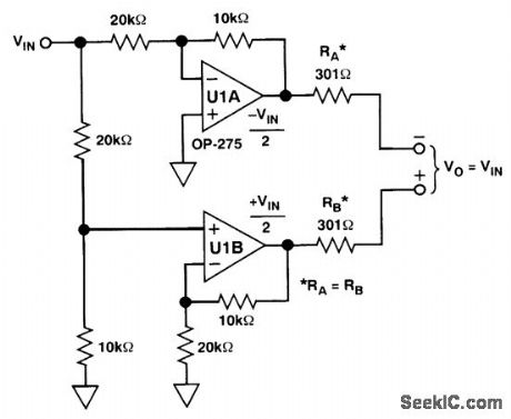
A line driver for 600 Ω can be configured from two IC op amps. U1A and U1B are Analog Devices OP-275. These devices feature low power consurrtption, low THD, and high slew rate. (View)
View full Circuit Diagram | Comments | Reading(1618)
MULTIPURPOSE_MINIAMPLIFIER
Published:2009/7/13 1:38:00 Author:May
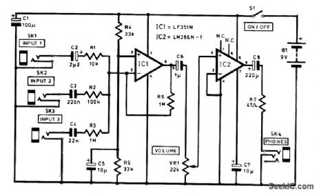
This circuit uses two audio IC amplifiers, one for a preamp and one for a power output stage. Three audio inputs are provided-low (1 mV), medium (10 mV), and high (100 mV) input-to drive a pair of headphones or a strtall speaker. The LM386 is good for 0.5 W or more output, and a small speaker can be connected directly to the junction of C8 and R7. A series combination of a 22-Ω resistor and a 0.1-mF capacitor should be connected between this point and ground to suppress possible high-frequency oscillations in this case. (View)
View full Circuit Diagram | Comments | Reading(1429)
AUDIO_POWER_BOOSTER
Published:2009/7/13 1:37:00 Author:May
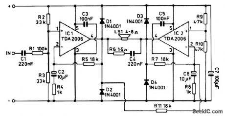
The audio power booster is based on two TDA2006 audio IC power amplifiers. Power amplifier IC1 is used as what is virtually a noninverting amplifier, with the noninverting input of the device beirtg biased to half the supply voltage by R2 and R3. R5 provides 100-percent negative feedback from the output to the inverting input of IC1 at dc so that the circuit has unity voltage gain and the output is biased to the required level of half the supply voltage. C2 and R4 remove some of the feedback at audio frequencies, and this gives a voltage gain of about 18 times at these frequencies. R1 is used at the input of the amplifier to reduce the sensitivity to a more suitable level, and C1 simply provides dc blocking at the input. IC2 is used in virtually the same configuration, but its noninverting input is not fed with an audio signal and it only receives the dc bias signal from R9 and R10. Resistor R11 couples the output signal of IC1 to the invertinginput of IC2, and the value of R11 is chosen to give IC2 an effective voltage gain of unity. However, as the input signal is coupled to IC2's inverting input, there is a phase inversion through this section of the amplifier, giving the required antiphase relationship at the two outputs. Diodes D1 to D4 are protection diodes for the two ICs, while R6 plus C4 helps to prevent instability. Components C3, C5, and C7 are all supply decoupling capacitors. (View)
View full Circuit Diagram | Comments | Reading(2885)
QUICK_SWITCHING_PNP_REGULATOR
Published:2009/7/13 1:36:00 Author:May
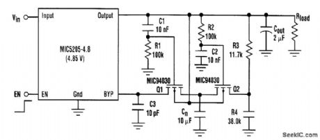
The MIC5205 is a low-dropout PNP regulator that incorporates a noise bypass pin for additional noise reduction. A single 10-nF capacitor, connected from the bypass pin to ground, reduces output noise by Vout/1.24 V (12 dB for the 5-V part) and creates a noise pole below 100 Hz. Switch-on time is increased from 80 μs to 15 ms. With the addition of a few components, the following circuit preserves a low switch-on time. A low-to-high signal on EN switches the output on quickly. This allows R1 and C1 to hold Q1 off while R2 and C2 hold Q2 on. Cn is also quickly charged to the bypass pin voltage through Q2 by the voltage divider R3, R4. C1 and C2 then charge to the output voltage,turntng Q1 on and Q2 off. Cn is now switched from the voltage divider to the bypass pin. The regulator is now in the low-noise configuratipn, which takes about 100 μs. When EN goes low, C1 and C2 discharge through R1, R2, R3, R4, and Rload. This resets the circuit for the next turn-on cycle. C3 helps prevent overshoot on the output. Ratio R3/R4 can be found empirically: First, set the ratio close to the ratio 1.24 V/(Vout-1.24 V), then adjust the value so the output turns on quickly without overshoot. The final tolerance needs to be 1 percent. Switch-off time is determined only by output capacitor size and the load. (View)
View full Circuit Diagram | Comments | Reading(1178)
MINI_MEGAPHONE
Published:2009/7/13 1:35:00 Author:May
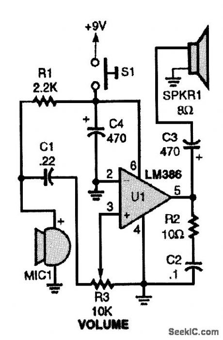
The mini megaphone is composed of an electret microphone (MIC1), an LM386 low-voltage audio-power amplifier (U1), a horn speaker (SPKR1), and a few other components. (View)
View full Circuit Diagram | Comments | Reading(5950)
The circuit using three switches to control a lamp
Published:2011/7/19 10:26:00 Author:Nancy | Keyword: three switches , a lamp
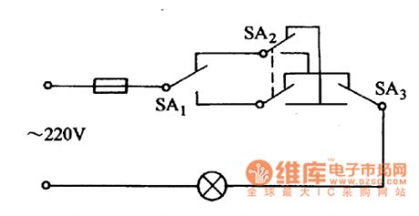
In some conditions, we need to control a lamp in three places, and at this time two single-pole double-throw switches and a double-pole-double-throw switch are needed, they are connected shown as the the figure. (View)
View full Circuit Diagram | Comments | Reading(888)
TEST_SEOUENCING
Published:2009/7/13 1:33:00 Author:May
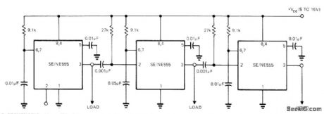
Uses 555 timers connected sequentially. With values shown, first timer runs for 10 ms after starting with pulse at terminal 2 or by grounding 2. At end of timing cycle, second circuit runs for 50 ms before triggering third circuit having 10-ms delay. Each timer controls its own load, as required for sequencing of automatic tester.-E. R. Hnatek, Put the IC Timer to Work in a Myriad of Ways, EDNMagazine, March 5, 1973, p 54-58. (View)
View full Circuit Diagram | Comments | Reading(2092)
| Pages:187/471 At 20181182183184185186187188189190191192193194195196197198199200Under 20 |
Circuit Categories
power supply circuit
Amplifier Circuit
Basic Circuit
LED and Light Circuit
Sensor Circuit
Signal Processing
Electrical Equipment Circuit
Control Circuit
Remote Control Circuit
A/D-D/A Converter Circuit
Audio Circuit
Measuring and Test Circuit
Communication Circuit
Computer-Related Circuit
555 Circuit
Automotive Circuit
Repairing Circuit