
Basic Circuit
Index 190
0_5_min_DELAY
Published:2009/7/12 23:27:00 Author:May
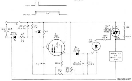
Value of resistor R controls duration of time delay provided by RCA 40841 dual-gate FET in SCR trigger circuit, with SCR in tum serving to triggertriacfor handling highcurrent resistive or inductive AC loads. Maximum delay of 5 min is obtained when R is 60 megohms (IRC type CGH or equivalent resistor). Timing is accurate within 10% over temperature rangeof -25℃to +60℃. D3 should be rated 60 V Use any SCR capable of handling triactrigger current,rated 60 V.- Linear Integrated Circuitsand MOS/FET,s, RCA Solid State Division,Somerville,NJ,1977,p435-437. (View)
View full Circuit Diagram | Comments | Reading(2258)
DIGITAL_LOGIC_FREQUENCY_DOUBLER
Published:2009/7/12 23:25:00 Author:May
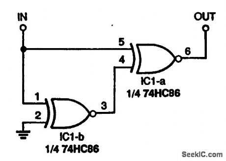
This circuit can be used if very high frequency operation is needed, or if very narrow output pulses can be tolerated. The output pulse width is determined by the propagation time delay of the exclusive-OR gate, and the input frequency cannot exceed 1/2(delay). (View)
View full Circuit Diagram | Comments | Reading(7177)
UHF_ATV_DOWNCONVERTER_FOR_900_AND_1300_MHz
Published:2009/7/12 23:18:00 Author:May
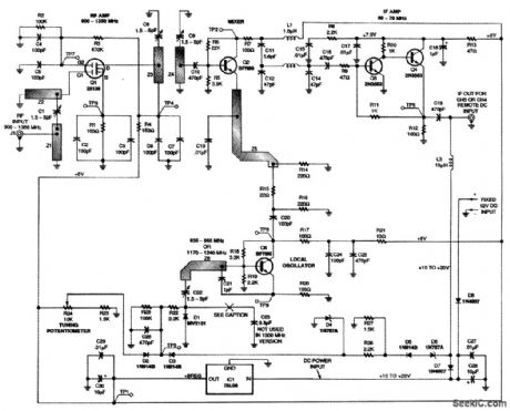
This clownconverter is tunable and can cover either 902 to 928 MHz or 1240 to 1300 MHz for receiving amateur television transmissions or other wideband signals. An NEO 25139low-noise RE am-plifier feeds a BFR90 mixer driven by a BFR tunable LO operating 61 or 67 MHz below the received frequency. A pair of 2N3563 transistors are used as a post-IF amplifier. Overall gain is 37 to 40 dB with around 1.5-dB noise figure. AGC control voltage can be used on gate 2 of the RF stage to reduce RF gain on strong signals; about -3 V is needed to reduce RE gain by >30 dB, Either on-board tun-ing via pot R24 or remote tuning via 10- to 20-V variable dc supply on the IF coaxial cable can be used. Note that striplines are different for 900 and 1300 MHz, and this requires separate models for each band, although the physical layout and circuit diagrams are identical.A complete kit of parts, including PC board, is available from North Country Radio, P.O. Box 53, Wykagyl Station, New Rochelle, NY 10804-0053A.
(View)
View full Circuit Diagram | Comments | Reading(1957)
Buck type converter circuit formed by the LT1766
Published:2011/7/27 9:58:00 Author:Nancy | Keyword: Buck type converter
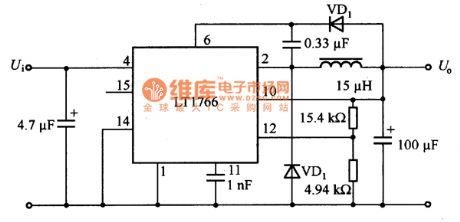
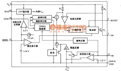
Figure a and b is the buck type converter circuit formed by the LT1766. It is a non-isolated buck type DC/DC converter with 5.5 ~ 60 V input voltage and 5 V / 1 A input. The LT1766 is a buck switch integrated regulator with all the functions that the buck type converter requires such as oscillating circuit, control circuit, switch transistor, etc. The oscillation frequency is 200 KHZ, the peak current of the on chip power transistors (VT1) is 1.5 A. (View)
View full Circuit Diagram | Comments | Reading(749)
FOUR_DIGIT_COUNTER
Published:2009/7/12 23:14:00 Author:May

A general-purpose four-digit counter can be made from a 74C925 IC and a few external components. That IC contains the counter, multiplexer, and seven-segment digit drivers, all in one convenient package. A couple of important notes about the circuit: The seven 220-Ω resistors (R1 to R7) are used as dropping resistors between the driver outputs and the segments of the display to protect the LEDs and keep the 74C925 from overheating. The four 2N3904 transistors (Q2 to Q5) act as amplifiers for the digital drivers to keep the display at full illumination. Switches S1 and 52, for reset and latch, respectively, are not crucial, but are highly recommended. The latch will freeze the count if needed. If the switches are not used, pin 12 needs to go to ground, and pin 5 to +V (the circuit's voltage supply). If more than four digits are needed, use the MM74C9261C. The functions are the same, but it has a carry out to cascade more than one chip and four-digit display. (View)
View full Circuit Diagram | Comments | Reading(8217)
12_V_TO_6_V
Published:2009/7/12 23:12:00 Author:May
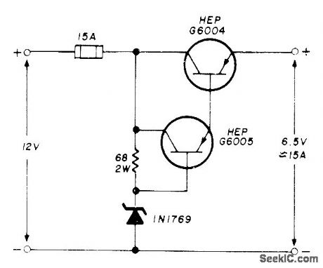
Permits operation of older 6-V VHF FM mobile equipment from 12-V storage battery. With transistor mounted on suitable heatsink, maximum output is 15 A. If positive and negative lines are isolated from chassis, converter may be used with either negative or positive ground.-E. Noll, Circuits and Techniques, Ham Radio, April 1976, p 40-43. (View)
View full Circuit Diagram | Comments | Reading(884)
FAlL_SAFE_TIMER_FOR_TRAlNS
Published:2009/7/12 23:12:00 Author:May
Provides delays up to 4 min, adiustable in 2-s steps, with accuracy better than 5%. Patented circuit was developed by ML Engineering to provide appropriate automatic braking or other action if engineer on train fails to respond to signal within period of delay.-W.E. Anderton,Computers,Communication and High Speed Railways,Wireless World, Aug,1975,p 348-353. (View)
View full Circuit Diagram | Comments | Reading(824)
Long time timing circuit formed by the LM106
Published:2011/7/27 9:49:00 Author:Nancy | Keyword: Long time timing circuit
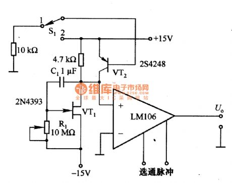
Figure 1 is the long time timing circuit formed by the LM106. The circuit is VT1 (FET tube) mueller integral circuit, if the gain of the circuit is A, the timing constant can be increased to A times. The gain of VT1 is about 60, the equivalent capacitance converted to VT1 grid is increased to 60 times, namely, 60 C1 is equal to 60 μF, and the maximum value of the grid resistance R1 is lOMΩ, so the timing can reach 6005. S1 is a reset switch, it resets when connects to 1 and VT2 conducts, C1 discharges through VT2 and resets to prepare timing for the next time. LM106 is a comparator circuit, the output is connected to corresponding circuit and for timing control. (View)
View full Circuit Diagram | Comments | Reading(683)
10_min_WITH_BLINKING
Published:2009/7/12 23:10:00 Author:May
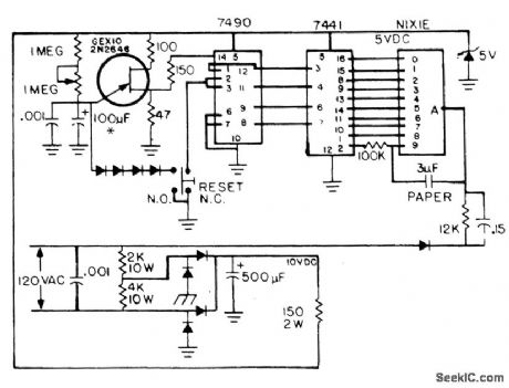
Station-identification timer uses single Nixie display to indicate elapsed time in minutes. After 9 min, numeral 9 blinks for 60 s before resetting to zero as visual reminder that amateur radio station identification should be made. Transistor can be GE X10 or 2N2646, Diodes are 1N4001 or equivalent. Numeral 9 or Nixie is connected as relaxation oscillator, flash rate of which can be changed by changing value of 100K resistor connected to pin 9.-W. Pinner, ID Timer, 73Magazine, Aug.1974, p 95-96.
(View)
View full Circuit Diagram | Comments | Reading(842)
EVENT_REGISTER
Published:2009/7/12 23:08:00 Author:May
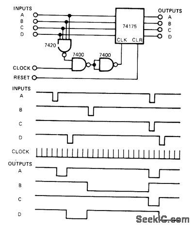
Inputs from sequential timer provide pulsed output and operate de-vices which stay on until next timed event. When an input goes low, output of four-input positive-NAND 7420 goes high, enabling the clock for 74175 4-bit D-type register. Since event-timer clock signal is used, outputs of register are coincident with clock. All outputs remain until one or more inputs goes low.-J. Glaab, Time Events with a Pulse Output Contrailer, EDNMagazine, Jan. 5, 1977, p 43. (View)
View full Circuit Diagram | Comments | Reading(1424)
WWV_TO_75_m_BAND_CONVERTER
Published:2009/7/12 23:04:00 Author:May
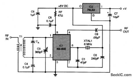
This circuit for an HP-band converter will convert the 10-MHz WWW signal to a frequency in the 75-m ham band. The local oscillator section of NE-602 is available on pins 6 (base) and 7 (emitter). In this circuit, a 6.00-MHz crystal oscillator is provided by the NE-602. Capacitors C1 and C2 form the feedback network. The junction of C2 and XTAL1 can be connected to either the 15-Vdc line or ground (the former is shown here). The difference frequency between WWV's 10 MHz and the 6.00-MHz crystal frequency is 4.00 MHz, which is located at the top end of the 75-m ham band. Crystals with other frequencies will produce other output sum or difference frequencies, so tune the receiver appropriately if something other than 6.00 MHz is used. (View)
View full Circuit Diagram | Comments | Reading(1453)
PARALLEL_INVERTER_DRIVE
Published:2009/7/12 23:04:00 Author:May
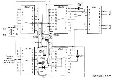
Uses Mullard modules for converting DC power to AC at high power levels for such applications as driving induction motors at higher speeds than are obtainable with line frequency. DC control voltage of 0-10 V varies output frequency up to 400 Hz.UPA61 modules provide functions of level detector, pulse generator, ramp generator, capacitor discharge circuit, and bistable MVBR for parallel inverter system. RSA61 and TT61 are trigger modules, with RSA61 also providing power supplies for other modules.- Universal Circuit Modules for Thyristor Trigger Systems (61 Series), Mullard, London, 1978, Technical Information 66, TP1660, p 19. (View)
View full Circuit Diagram | Comments | Reading(1044)
UP_DOWN_COUNTER_WITH_XOR_GATES
Published:2009/7/12 23:02:00 Author:May
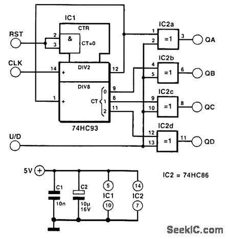
This circuit shows how a regular 4-bit binary counter can be extended with an up/down function just by adding four XOR (exclusive-OR) gates. The principle is simple: The level at the common in-puts of the XOR gates determines whether the gates invert the counter's QA to QB output levels or not. In this way, the outputs of the XOR gates can be made to cycle from 1111 dowtt to 0000 instead of from 0000 to 1111. The disadvantage of this circuit over a real up/down counter is the jump, which occurs when the level on the U/D control input is changed. The sum of the old state and the new state is always 15. For example, if the counter is at state 3 in count-up mode, the state becomes 12 when the U/D line is made logic high to initiate down counting. (View)
View full Circuit Diagram | Comments | Reading(1933)
SIMPLE_FREQUENCY_DOUBLER
Published:2009/7/12 23:02:00 Author:May
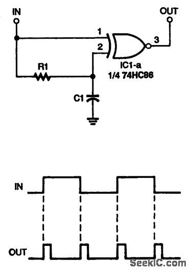
This circuit uses only a single exclusive-OR gate and a couple of passive components. The width of the output pulses is determined by the time constant of the RC network,and the maximum input frequency cannot exceed 1/2RC. (View)
View full Circuit Diagram | Comments | Reading(4977)
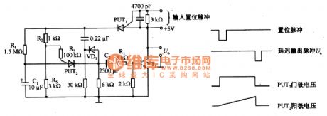
Timing circuit formed by PUT
Published:2011/8/2 19:44:00 Author:Nancy | Keyword: Timing circuit, PUT
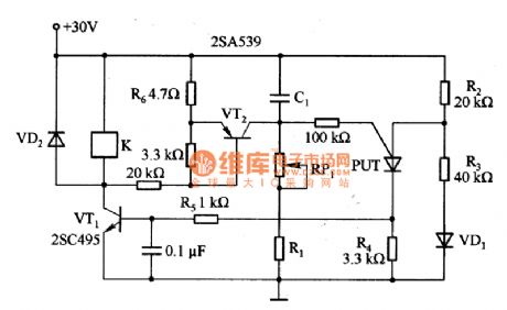
Figure 1 is the timing circuit formed by PUT. It is a 0.5s一lmin time variable timing circuit composed by PUT. The anode-cathode of PUT is offset by the voltage division of fixed resistors R2 and R3, the timing is decided by the capacitor C1 and resistor (R(RP1)十R1) connected to the gate. The base current of the drive transistor VT1 of the relay K is decided by the R2, R4 and R5, it is not relevant to the timing setting resistor for the PUT conduction. The electric charge of capacitor C1 discharges through VT2 and R6, the diode VD1 used to compensate the temperature characteristic of PUT. (View)
View full Circuit Diagram | Comments | Reading(722)
10_dB_50_W_ATTENUATOR
Published:2009/7/12 22:54:00 Author:May

The 10-dB attenuator has an attenuation of 10 dB at lower frequencies at 2 m and 70 cm; circuit losses increase to 10.8 dB and 12.0 dB, including interconnecting RG-58/U cable losses of 0.4 dB and 0.6 dB, respectively. Establishing an SWR of less than 1.1:1 at 70 cm was the most crucial design consideration. Changes occur with different coolants. If the assembly is tailored for minimum SWR in air, its SWR increases to about 1.3:1 when you put it in vegetable oil. The SWR changes are caused by increased circuit capacitance due to the dielectric. This condition was improved by using household wax, paraffin, instead of oil. Cctution: Paraffin has ct relatively Lou;ftctsh temperature; it can be used to make candles. Next, to decrease the circuit distributed capacitance, increase the distance of the components from the circuit board by stacking two layers of PC boards at the tie-down pads.This raises the parts of connecting positions to about 0. 120 in. The completed assembly has an SWR of less than 1. 1 : 1 at both 70 cm and 2 m. Schematic and layout of the 10-dB attenuator: R1, 10-Ω 1/2-W (7); R2, 1-kΩ 1/4 W (14). A. Input/output, 3 ft RG-58/U. B. Cable bushing, 1/4 in. clearance hole. C. Component mounting board, 3 1/2 inX23/8 inX1/14, in PCB. D. Fan out end cable braid, twist into two segments, and solder to PCB with ntinimum lead lengths. E. Component tie-down pads (9), double thickness glass-epoxy PCB, 1/4inX1/8 inX1.8 in pieces cemented together and into position with clear household cement (Elmer's). F. Coolant, household wax (paraffin). Fill container with melted wax to 1/4 in from the top. To melt wax, insert the container in hot water (about 200°F). G. Container, one-pint can. (View)
View full Circuit Diagram | Comments | Reading(1014)
VOLTAGE_CONVERTER
Published:2009/7/12 22:52:00 Author:May
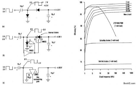
This bootstrap voltage converter begins with the basic diode inverter circuit (a). Placing a MOSFET across each diode will improve efficiency (b). The final step involves using a single noninverting CMOS digital gate to replace the diodes (c).The performance curves depict the bootstrap voltage converter's efficiency, which is 99 percent from 5 to 500 kHz using 10-μF capacitors and a 1-mA load. A typical commercial unit operates at only 94 percent efficiency. (View)
View full Circuit Diagram | Comments | Reading(1189)
30s timing circuit formed by PUT
Published:2011/8/2 10:11:00 Author:Nancy | Keyword: 30s timing circuit, PUT
If you add a set pulse between the cathode-anode of PUT1, then PUT conducts, the + 5 V power supply charges C1 through it, the voltage of C1, which is the anode voltage of PUT2, increases gradually. When the anode voltage is higher than the gate bias voltage, PUT2 conducts, the discharging current of C1 flows through the drive transistor VT1 to make it saturate and conduct, the output Uo is close to OV. The C1 voltage add a reverse bias to PUT1, PUT1 cuts off to make the circuit reset. The output pulse width is basically decided by the C2 and R1, the pulse width is about 10 us. The delay time of the output pulse is decided by the R2, R3, R4 and C1. (View)
View full Circuit Diagram | Comments | Reading(652)
MULTISWITCH_CHARGE_PUMP_BOOST_CONVERTER
Published:2009/7/12 22:47:00 Author:May
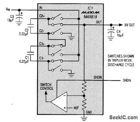
This device is useful both in main supplies and in backup supplies. It generates a regulated 5-V output for load currents to 20 mA and inputs ranging from 1.8 to 3.6 V. For input voltages no lower than 3 V, the output current can reach 50 mA. The circuit accomplishes regulation without a linear pass element, but its losses are the same as those of an unregulated doubler or tripler feeding into a linear regulator. (View)
View full Circuit Diagram | Comments | Reading(830)
RATIOMETRIC_20_kHz_V_F_CONVERTER
Published:2009/7/12 22:46:00 Author:May
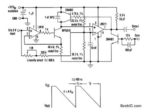


This ratiometric 20-kHz voltage-to-frequency converter (VFC) provides superior perforrnance with strain gauges and other ratio-responding transducers-even with noisy, unregulated excitation voltages. Feedback isn't used to achieve the excellent 4-Hz linearity, so there is very-low-frequency jitter-period measurements can be used to get several digits of resolution- even when operating at a fraction of full scale. An optional synchronizing transistor starts the VFC with zero charge at the beginning of each count cycle, eliminating the characteristic digit-jumping often encountered with VFC designs. Grood linearity is attained by making the comparator's reference voltage vary with the input voltage, which precisely compensates for the finite capacitor reset time:where AVin△V/△t. If Vref is made to include the amount t1AVin, then the effect of t1 is elirninated:The MPSA18 is a remarkably high-gain transistor, even at low currents, producing good current-source linearity down to 0 Hz. In addition, bipolar transistors work well with the low collector voltages encountered in this single-supply 10-V design. Moreover, most single-supply op amps will work in place of the LM10. But the LM10 also has a reference amplifier that could be used to construct a 10-V excitation regulator. The LM311 propagation delay gives a reset pulse width near 400 ns, which gives the transistor time to discharge the capacitor. Also, the 311's bias current produces a small negative offset that ensures a 0-Hz output for Vin. (View)
View full Circuit Diagram | Comments | Reading(935)
| Pages:190/471 At 20181182183184185186187188189190191192193194195196197198199200Under 20 |
Circuit Categories
power supply circuit
Amplifier Circuit
Basic Circuit
LED and Light Circuit
Sensor Circuit
Signal Processing
Electrical Equipment Circuit
Control Circuit
Remote Control Circuit
A/D-D/A Converter Circuit
Audio Circuit
Measuring and Test Circuit
Communication Circuit
Computer-Related Circuit
555 Circuit
Automotive Circuit
Repairing Circuit