
Basic Circuit
Index 186
74HCT4538N double precision monostable multivibrator integrated circuit
Published:2011/7/27 10:26:00 Author:Nancy | Keyword: double precision , monostable multivibrator
The 74HCT4538N is a double precision monostable multivibrator integrated circuit widely used in TV, audio, VCD, computers and monitors, and other electrical equipment.
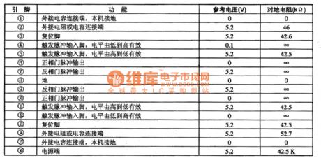
The 74HCT4538N integrated circuit includes two monostable multivibrators with the same function inside. It can replace directly the model CC4538β. The IC uses DIP package widely used in the BaiHong DT2000 type frequency doubling wide screen color TV. The pin function and data is shown as table 1. (View)
View full Circuit Diagram | Comments | Reading(635)
EMITTER_COUPLED_MVBR
Published:2009/7/16 5:03:00 Author:Jessie
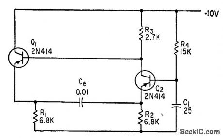
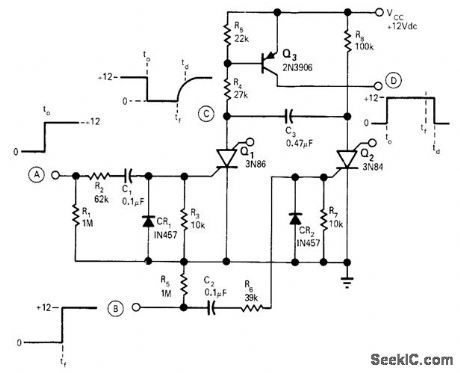
When Q1 conducts, Q2 is cut off and conversely. Duration of both quasi-stable states is controlled by Ce. Q2 should saturate when conducting, to prevent distortion in flat tops of rectangular output pulses.-B. Rakovic, One More Transistor makes a Linear Sawtooth, Electronics, 35:49, p 50-51. (View)
View full Circuit Diagram | Comments | Reading(707)
Digital integrated circuit diagram
Published:2011/7/13 9:50:00 Author:Nancy | Keyword: Digital integrated circuit
The digital circuit has some advantages: (1)high stability; (2)processing precision is not limited by the pin; (3)logical calculus and judgement function; (4)digital information can be stored for long time, etc. The above advantages of the digital circuit make the digital integrated circuit develop rapidly. Now the digital integrated circuit has been widely used in the national economy and people's life and is expanding its range of application in a high speed. (View)
View full Circuit Diagram | Comments | Reading(534)
MEMORY_DRIVER
Published:2009/7/16 5:00:00 Author:Jessie
Extract-driver circuit furnishes current to extract information from random-access memory of Burroughs B-251 Visible Record Computer.-G. E. Lund and D. R. Faulis, Expandable Random Access Memories, Electronics, 33:11, p 164-166. (View)
View full Circuit Diagram | Comments | Reading(684)
Improving load capacity circuit diagram
Published:2011/7/15 10:01:00 Author:Nancy | Keyword: load capacity
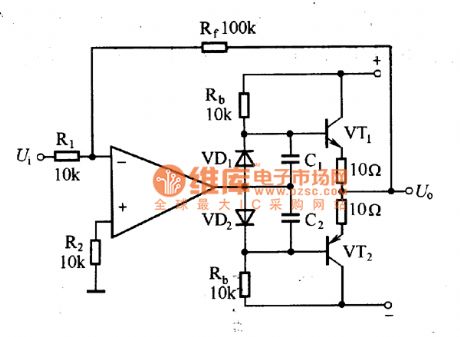

The load capacity of the general integrated operational amplifier load ability is weak, it only allows for dozens of mV power consumption, the maximum output current is also only 10 mA. So, when need large load voltage or current, you need add circuit with extended function at its output pin.
The circuit shown as figure a is a circuit using complementary push-pull output to expand current. When Ui = 0, Uo = 0, the current flows through the base loop of Rb, VD1, VD2 and VT1,VT2 and it provides bias current to VT1 and VT2, which makes it work in A B amplification state and reduce crossover distortion. The weakness of the circuit is that it can't raise voltage range.
The circuit shown as figure b is a circuit which can expand current and voltage range. (View)
View full Circuit Diagram | Comments | Reading(781)
95_PERCENT_EFFICIENT_5_V_INPUT_33_V_OUTPUT_DC_TO_DC_CONVERTER
Published:2009/7/13 2:36:00 Author:May
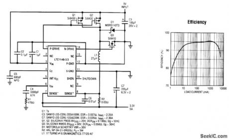
Computing equipment increasingly requires both 3.3-V and 5-V logic supplies, with only the 5-V being readily available. As 3.3-V current demands increase to include microprocessors, coprocessors, DSP processors, and memory, the total power demands on the 3.3-V supply rule out the rela-tively low efficiency and high dissipation of a linear regulator. The circuit shown here supplies 5 A at 3.3 V with over 94-percent efficiency by using the LTC1148-3.3 synchronous switching regulator.This surface-mount solution (L1 is through-hole) requires no heatsinks and very little board space.High efficiency is also maintained at low output currents by implementing Burst mode operation, making the LTC1148-3.3 solution ideal for supplies using normal/sleep modes, such as those in Green PCs. The LTC1148-3.3 can be placed in a shutdown mode, reducing supply current to a mere 22μA. (View)
View full Circuit Diagram | Comments | Reading(673)
DIGITAL_STOPWATCH
Published:2009/7/13 2:35:00 Author:May
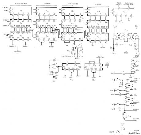
Provides 41/2-digit liquid crystal display for up to 19 min 59.9 s, after which tens of minutes stays at 1 and unit digit recycles from 0 to 9, Gives over 600 hours continuous operation from 5-V mercury battery. Accuracy is determined by 100-kHz crystal oscillator, output of which is divided in two dual decade counters to provide 50-Hz display drive and 10-Hz timing signal. ICs 1, 2, 3, 4, 16, and 17 ai'e CD4518; 5-8 are CD4019; 9-13 are CD4056; 18and 19 are CD4011. Article gives construction and operation details.-P. A. Bimie, Digital EventTimer, Wireless World, Part 1-Dec. 1976, p 32-34 (Part 2-Jan. 1977, p 65-68). (View)
View full Circuit Diagram | Comments | Reading(2415)
Tone circuit diagram made by LM1036
Published:2011/7/15 10:58:00 Author:Nancy | Keyword: Tone
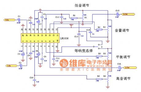
LM1036 is a voltage controlled double channel, tone (high/low), volume, left and right volume adjustment IC. It has a loudness switch to compensate the ear characteristic curve when the volume is small. Because it is controlled and adjusted by the voltage, it can use the single-chip microcomputer control circuit to adjust tone, volume, balance and equal loudness, and can not use the offensive duplex (or single) potentiometer completely, and this can't effect the tone quality even using it. (View)
View full Circuit Diagram | Comments | Reading(4552)
9_V_INPUT±5_V_OUTPUT_DC_TO_DC_CONVERTER
Published:2009/7/13 2:31:00 Author:May
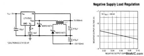
Many dc-to-dc converter applications require regulated complementary output voltages from a single loosely regulated source. A common use for this is supplying 5 V and -5V to a video op amp for amplification or cable driving. Accomplishing this task in a space-effective manner with a minimum of corrtponents is a challenge for a designer. The LT1176-5 circuit shown here uses a single integrated switching regulator and an off-the-shelf inductor with an extra winding to generate ±5 V from an 8- to 12-V input. The circuit is designed to supply 5 V as the main output with up to 800 mA of load current, and -5 V as a secondary output with up to 100 mA load current. Regulation is adequate for most opamp circuits: 5-V regulation will be ±3 percent and -5-V regulation is about ±10 percent for loads between -10 and -100 mA. The LT1176-5 providesacomplete 100-kHz switching regulator with a 1.2-A on-chip switch in a thin 20-lead SO package. The enhanced thermal characteristics of the fused-lead SO package allow higher power outputs than were previously possible with SOs. (View)
View full Circuit Diagram | Comments | Reading(877)
OP_AMP_RESPONSE_NULL_CIRCUIT
Published:2009/7/13 2:28:00 Author:May
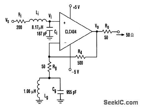
A sharp null can be achieved in a current feedback op amp's frequency response by adding a sharp cutoff filter. The response is modified by adding a resonant circuit in series with the gain-setting resistor Rg. (View)
View full Circuit Diagram | Comments | Reading(729)
TIMER_WITH_MEMORY
Published:2009/7/13 2:27:00 Author:May
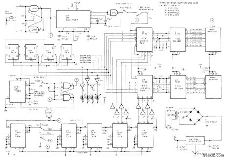
Time elapsed since initial triggering at start of event is shown on 2digit MAN-1 display in seconds or tenths of seconds and written into memory, Up to 16 event times can be stored for later readout. Free-running mode counts off seconds or tenths of seconds on display. Article covers construction and operation. Circuit was Science Fairwinner. Gate and opamp types are not critical.-M. Event Timer with Memory.73 Magazine, 1977,p 72-74. (View)
View full Circuit Diagram | Comments | Reading(1070)
200_W_AT_25_kHz
Published:2009/7/13 2:26:00 Author:May
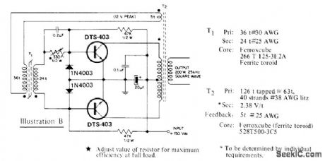
Two Deleo DTS-403 highvoltage silicon transistors are connected as push-pull oscillator operating on 150-VDC bias.Efficiency is 78% at full load. Diodes serve alternately as steering and clamp diodes.- 25 kHz High Efficiency 200 Watt Inverter, Deleo, Kokomo, IN, 1971, Application Note 47. (View)
View full Circuit Diagram | Comments | Reading(2996)
TWO_INDEPENDENT_DELAYS
Published:2009/7/13 2:26:00 Author:May

Each timer section of Exar XR-2556 dual timer operates independently in mono MVBR mode to provide delays shown above output waveforms Supply voltage range is 4.5 to 16 v.-Timer DataBook, Exar Integrated Systems, Sunnyvale,CA,1978,p23-30. (View)
View full Circuit Diagram | Comments | Reading(621)
1_min_WITH_TRANSISTOR_ARRAY
Published:2009/7/13 2:24:00 Author:May
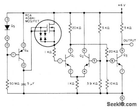
Circuit uses RCA CA3096AE five-transistor array in combination with dual-gate MOSFET to provide timing action that maintains accuracy within 7% for supply voltage variations of ±10%, Q5 is one of PNP transistors connected as diode.- Linear Integrated Circuits and MOS/FET's, RCA Solid State Division, Somerville, NJ, 1977, p 205-210. (View)
View full Circuit Diagram | Comments | Reading(904)
LOW_STANDBY_DRAIN
Published:2009/7/13 2:23:00 Author:May
Positive 12-V pulse at input A triggers SOS Q1 and turns on transistor switch Q3, Positive pulse at input B gates SCS Q2 on and turns off Q3. Current drain is essentially zero (typically 3 μA). Circuit was designed to supply up to 7 mA of switched current from 12-VDC supply.-D. B. Heckrnan, Bistable Switch with Zero Standby Drain, EDN|EEE Magazine, Oct. 1, 1971, p 42. (View)
View full Circuit Diagram | Comments | Reading(710)
CAR_STEREO_SUBWOOFER_CROSSOVER
Published:2009/7/13 2:21:00 Author:May
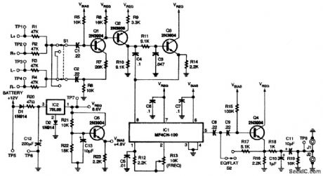
This figure is the schematic for the subwoofer crossover. The inputs through Q1 form a differential summing amplifier, with switch S1 functioning as a polarity inverter. A 24-dB-peroctave switched capacitor filter (IC1) is the heart of the continuously variable filter. Potentiometer R13 controls the cutoff frequency of IC1 by controlling its sampling frequency. Because of the in-herent sampling action of switched capacitor filters, an antialiasing filter is required at the input of IC1. Transistors Q2 and Q3, along with the surrounding components, form this second-order low-pass antialiasing filter. The subsonic filter with a boost stage follows the output of IC1 at 5. When switch S2 is closed, the boost is added. Additional subsonic filtering action is provided by C1 and C2 at the inputs of the crossover circuit. A reconstruction filter that eliminates sampling artifacts is formed by R18 and C10 at the output of IC1. The power-supply circuit, based on the 78L08 voltage regulator (IC2), provides both an 8.6-V main supply and a 4.8-V bias supply. Diode D1 protects against negative voltage spikes and incorrect hookup. Diode D2 biases the 78L08 regulator reference pin at 0.6 V to provide an output of 8.6 V, rather than 8 V. (View)
View full Circuit Diagram | Comments | Reading(2661)
HIGH_GAIN_AMPLIFIER_FOR_PHOTODETECTORS
Published:2009/7/13 2:19:00 Author:May
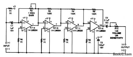
Suitable for photodetectors, laser experiments, or general use, single LM324 quad op amp. A 9-V supply is recommended. (View)
View full Circuit Diagram | Comments | Reading(1491)
HIGH_CURRENT_5_V_TO_12_V_25_A_DC_TO_DC_CONVERTER
Published:2009/7/13 2:16:00 Author:May
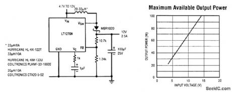
Many applications require a 12-V supply for control, data storage, interface, or driver functions.These designs often require high peak currents, and a 12-V supply might not be available with high enough current. The LT1270A circuit shown here will provide a minimum of 2.5 A at 12 V from a 5 V ±5 percent supply. The LT1270A has a 10-A high-efficiency switch and a low 10-mA (maximum) supply current, which provides excellent efficiency in high-current-output dc-to-dc conversion circuits. The 60-kHz swttcittng frequency has been optimized for best efficiency. (View)
View full Circuit Diagram | Comments | Reading(783)
REMOTE_DIGITAL_PROGRAMMING_OF_TIMER
Published:2009/7/13 2:16:00 Author:May
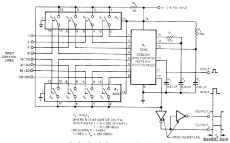
Either binary or BCD logic can be used for selecting delay interval of monostable timer A1, with delays being integral multiples of shortest time. Timing is programmed by pair of 4016 CMOS analog switches, A2 and A3. Given timing tap is activated when corresponding digital input control line is high and deactivated when control is low. Programmable timing range is 1 to 255 ms for 2240, and 1 to 99 ms for 2250 or 8250 timer. Basic interval can bechanged to suit other applications. CMOS output buffer stage ensures valid output logic Ievels. Although circuit will operate over supply range indicated, operation is optimum forsupply of 10 to 15V.-W. G. Jung, Take a Fresh Look at New IC Timer Applications, EDN Magazine, March 20, 1977, p 127-135. (View)
View full Circuit Diagram | Comments | Reading(855)
Voltage negative feedback offset circuit diagram
Published:2011/7/18 10:36:00 Author:Nancy | Keyword: negative feedback, offset circuit
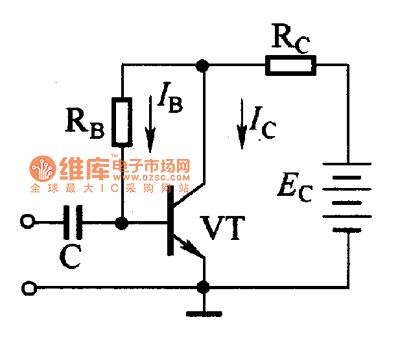


The voltage negative feedback offset circuit is shown as the figure. The bias resistor RB is connected to the transistor collector, which is the difference between it and the fixed offset circuit. At this time the parameters in the circuit has the following relations:
Because the UBE is very small and can be ignored, at this time
The process of steady working point of the circuit is as below:
From the above process, you can see that the change of IC is back along with the increase of temperature, which realizes the role of stabilizing the static working point.
To make the the effect of the circuit excellent, you must make RC large enough, only this can cause the UCE change much and deepen the effect of the voltage negative feedback. So this circuit is not suitable for the circuit which uses the transformer as load. Drift resistance value (2~ 1 O) is often chosen as Rc. (View)
View full Circuit Diagram | Comments | Reading(842)
| Pages:186/471 At 20181182183184185186187188189190191192193194195196197198199200Under 20 |
Circuit Categories
power supply circuit
Amplifier Circuit
Basic Circuit
LED and Light Circuit
Sensor Circuit
Signal Processing
Electrical Equipment Circuit
Control Circuit
Remote Control Circuit
A/D-D/A Converter Circuit
Audio Circuit
Measuring and Test Circuit
Communication Circuit
Computer-Related Circuit
555 Circuit
Automotive Circuit
Repairing Circuit