
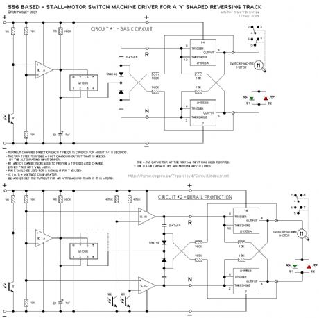
Basic Circuit
Index 27
Flip-Flop circuit
Published:2013/6/21 3:02:00 Author:muriel | Keyword: Flip-Flop circuit
View full Circuit Diagram | Comments | Reading(894)
OUT-AND-RETURN OPERATION
Published:2013/6/21 3:01:00 Author:muriel | Keyword: OUT-AND-RETURN OPERATION
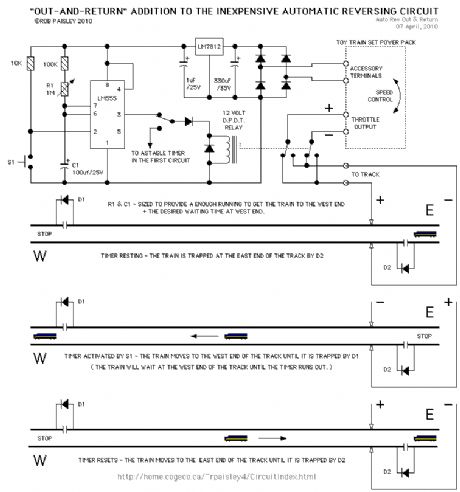
In this circuit the train only moves when S1 is pushed. After a set waiting time the train returns to its start position and then waits.
The 555 timer in this circuit is configured as a monostable oscillator. The SPDT switch allows the circuit to be changed from normal operation to out-and-back operation. Two 555 timers are indicated but a 556 timer can also be used. (View)
View full Circuit Diagram | Comments | Reading(744)
longer stopping sections
Published:2013/6/21 2:59:00 Author:muriel | Keyword: longer stopping sections
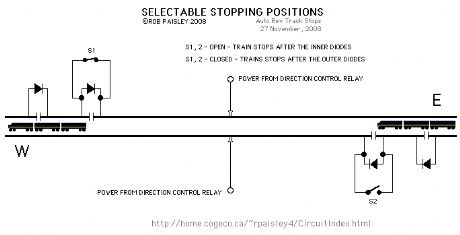
The next diagram shows how to provide increased stopping distances for trains with head-end power. The longer stopping sections can be switched if the train is reversed. (View)
View full Circuit Diagram | Comments | Reading(846)
BASIC TRACK CIRCUIT
Published:2013/6/21 2:59:00 Author:muriel | Keyword: BASIC TRACK CIRCUIT
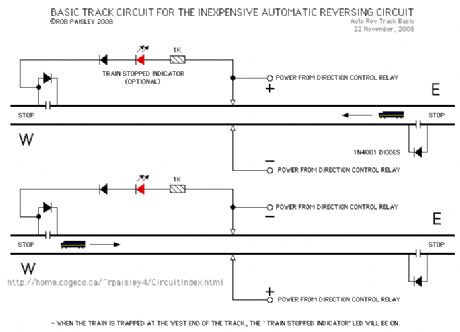
The basic track circuit provides continuous back and forth operation of the train with diodes and gaps to stop the train at each end of the track.Also shown is an optional LED that will show when the train has been trapped at the end of the track. (View)
View full Circuit Diagram | Comments | Reading(1121)
POWER SUPPLY and TIMER
Published:2013/6/21 2:58:00 Author:muriel | Keyword: POWER SUPPLY and TIMER
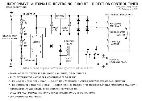
The power supply circuit provides power to the track and has a 12 volt power source for the 555 timer IC that controls the waiting time at each end of the track.
NOTE: The circuit does not know when or how fast the train is moving, therefore the timer's cycle times must also include the time for the train to travel along the track in either direction. For example it the train is to wait for 30 seconds at the end of the track, the timer will be set for: The time to travel to the end of the track + 30 seconds.The reversing switch on the power pack itself is only used to set the initial travel direction of the system or to 'switch ends' if the waiting times are not equal.
The calculator at the following link can be used to determine values for resistors R1 and R2 and capacitor C1. (LM555 - Astable Oscillator Calculator)
(View)
View full Circuit Diagram | Comments | Reading(839)
CURRENT LIMITING RESISTOR CALCULATOR FOR LIGHT EMITTING DIODES
Published:2013/6/21 2:52:00 Author:muriel | Keyword: CURRENT LIMITING RESISTOR CALCULATOR , LIGHT EMITTING DIODES
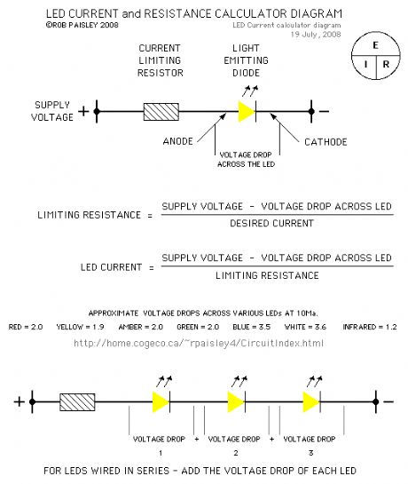
The calculators on this page can be used to find current limiting resistors and currents for Light Emitting Diodes.
The first calculator determines the resistance for a desired LED current while the second calculates the current for a given resistance. (View)
View full Circuit Diagram | Comments | Reading(1012)
Block Occupancy Detector Helper Circuit
Published:2013/6/21 2:52:00 Author:muriel | Keyword: Block Occupancy Detector, Helper Circuit
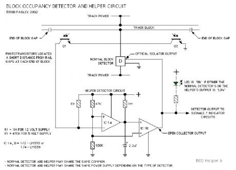
This circuit would be used to hold a BLOCK OCCUPIED condition as a train passes out of the block even if the normal detector is not sensing a train.
The Helper circuit uses phototransistor type light activated detectors to sense that a train is still in the block, even though the engine has left that block.
The only reason to use this circuit is if there are no conducting wheel sets at the tail end of the train that would keep the normal occupancy detector activated until the train has completely exited from the block.
Simply stated the Helper circuit's output is in parallel with that of the normal detector. When the Helper circuit is activated by a train covering one of the phototransistors at either end of the block, the Helper's output holds the block as occupied even though there is no current flowing through the sensing circuit of the normal detector and has therefore turned OFF. (View)
View full Circuit Diagram | Comments | Reading(936)
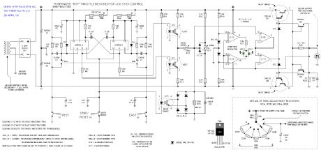
Joy Stick Controlled - Modernized "Toy" Throttle Mk.2 Circuit
Published:2013/6/21 2:49:00 Author:muriel | Keyword: Joy Stick Controlled , Modernized "Toy", Throttle, Mk.2 Circuit
View full Circuit Diagram | Comments | Reading(872)
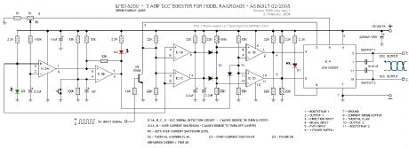
3Amp - DCC Booster Circuit #1
Published:2013/6/21 2:48:00 Author:muriel | Keyword: 3Amp , DCC Booster Circuit

View full Circuit Diagram | Comments | Reading(736)
MiniDCC© H-Bridge Circuit
Published:2013/6/21 2:47:00 Author:muriel | Keyword: MiniDCC© H-Bridge Circuit
View full Circuit Diagram | Comments | Reading(577)
MiniDCC© Circuit Board Connection Diagram
Published:2013/6/21 2:47:00 Author:muriel | Keyword: MiniDCC©, Circuit Board, Connection Diagram
View full Circuit Diagram | Comments | Reading(1007)
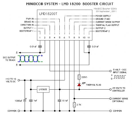
The 3 Amp Booster For My MiniDCC© System
Published:2013/6/21 2:45:00 Author:muriel | Keyword: 3 Amp, Booster, MiniDCC© System
The following schematic is for the booster that was built for my MiniDCC® System. Designed around an LMD 18200 H-Bridge. The circuit includes signal failure detector and over current protection that will remove power to the tracks should either activate.
The signal detector will automatically clear itself but the over-current detector must be manually reset.
(View)
View full Circuit Diagram | Comments | Reading(917)
Zero Stretching Of DCC Voltages
Published:2013/6/21 2:44:00 Author:muriel | Keyword: Zero Stretching , DCC Voltages
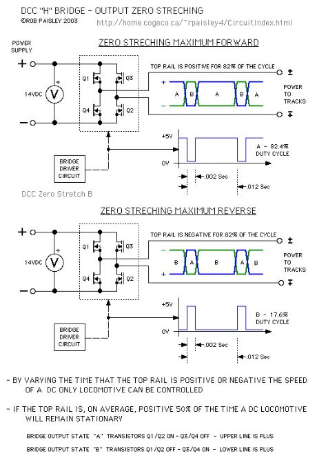
The next diagram shows a very simplistic explanation to Zero Stretching as it applies to DCC systems.
As in the above diagrams the rate at which the voltage changes polarities has not been considered. The important factor in Zero Stretching is the average time that the voltage to the track is either positive or negative.
(View)
View full Circuit Diagram | Comments | Reading(694)
Full Wave Rectification
Published:2013/6/21 2:42:00 Author:muriel | Keyword: Full Wave Rectification
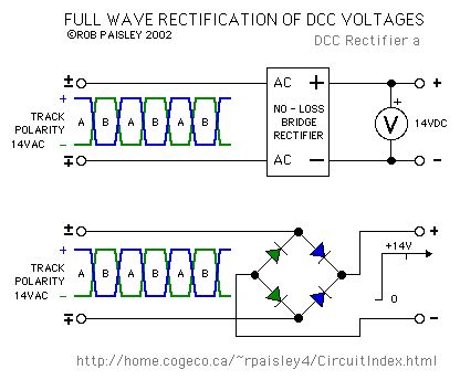
The next diagram shows the effect of rectifying a DCC voltage with a full wave bridge. The voltage at the output of the bridge is equal to the input minus the drop across the diodes.
The small tick in the output of the bridge occurs when the polarity of the H-Bridge reverses. The size of the ticks is largely determined by the efficiencies of the H-Bridge and rectifier bridge and in most cases can be ignored. This is why filter capacitors are not needed for decoders.Diodes used to rectify DCC should be Schottky or high speed silicon types. Diodes of the 1N4000 and 1N5400 series are not suitable for this application due to their slow turn-off times. (View)
View full Circuit Diagram | Comments | Reading(854)
Basic Half Wave - DCC H-Bridge Circuit
Published:2013/6/21 2:41:00 Author:muriel | Keyword: Basic Half Wave , DCC H-Bridge Circuit

The next schematic shows a Half DCC H-Bridge circuit in a very basic form. The reversing switch has now been replaced by two transistors that are alternately switched ON and OFF.
Oscilloscopes A and B are not relevant to this circuit as the output of the bridge is actually referenced to the common of the power supply.
The waveform for the C oscilloscope above does apply to this circuit and illustrates why a 28 volt signal appears at the output while the instantaneous voltage does not exceed one half of the maximum supply voltage.
(View)
View full Circuit Diagram | Comments | Reading(1348)
Basic DCC Full H-Bridge Circuit
Published:2013/6/21 2:41:00 Author:muriel | Keyword: Basic DCC Full H-Bridge Circuit
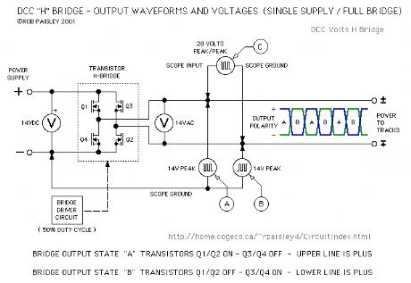
The next schematic shows a Full Wave - DCC H-Bridge circuit in a very basic form. The DPDT reversing switch has been replaced by four transistors connected in pairs that are alternately switched ON and OFF.
Oscilloscopes have been added to the circuit in order to show what the waveforms would look like at various points in the system. Illustrations explaining the waveforms follow this diagram. (View)
View full Circuit Diagram | Comments | Reading(1015)
DCC Bridge Mimic Circuits
Published:2013/6/21 2:41:00 Author:muriel | Keyword: DCC Bridge Mimic Circuits
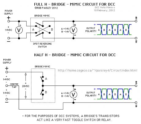
The first diagram illustrates the basic function of full and half H-Bridge circuits as used for model railroad DCC booster systems. (View)
View full Circuit Diagram | Comments | Reading(921)
Meter Placement Diagram
Published:2013/6/21 2:39:00 Author:muriel | Keyword: Meter Placement Diagram
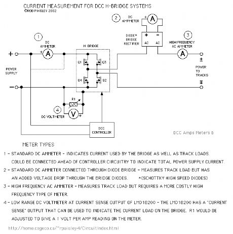
The following diagram shows a very simple schematic of an H-Bridge circuit with current indicating meters placed at various locations.
Text on the diagram indicates the type of meter and any special considerations involved. (View)
View full Circuit Diagram | Comments | Reading(772)
Flashing Rear-End Device For DCC
Published:2013/6/18 21:39:00 Author:muriel | Keyword: Flashing, Rear-End Device, DCC
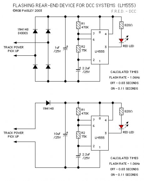
View full Circuit Diagram | Comments | Reading(944)
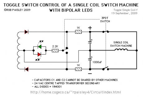
Controlling Single Coil Switch Machines 4
Published:2013/6/18 21:38:00 Author:muriel | Keyword: Single Coil, Switch Machines
View full Circuit Diagram | Comments | Reading(739)
| Pages:27/471 At 202122232425262728293031323334353637383940Under 20 |
Circuit Categories
power supply circuit
Amplifier Circuit
Basic Circuit
LED and Light Circuit
Sensor Circuit
Signal Processing
Electrical Equipment Circuit
Control Circuit
Remote Control Circuit
A/D-D/A Converter Circuit
Audio Circuit
Measuring and Test Circuit
Communication Circuit
Computer-Related Circuit
555 Circuit
Automotive Circuit
Repairing Circuit