
Index 99
SCR_LATCHING_CIRCUIT_WITH_RATE_EFFECT_SUPPRESSION
Published:2009/7/15 23:09:00 Author:Jessie
With basic scr latching circuit (at left) for latching on lamp when input voltage level is exceeded, resetting of circuit by opening supply lead exposes scr to fast transients and possible turn-on due to rate effect. Adding 100,000-ohm resistor and using four-terminal silicon controlled switch suppresses rate effect.-R. A. Stasior, How to Suppress Rate Effect in PNPN Devices, Electronics, 37:2, p 30-33. (View)
View full Circuit Diagram | Comments | Reading(1323)
120_V_A_C_LATCH
Published:2009/7/15 23:06:00 Author:Jessie
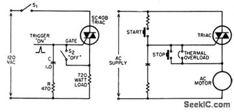
Bidirectional controlled rectifier (G.E. Triac) replaces more complicated scr or power transistor circuits for static switching of a-c power circuits. Can be adapted to simulate action of magnetic starter for a-c motor Momentary closing of start switch (in circuit at right ) latches Triac on and starts motor-F. W. Gutzwiller, Simplified 120 VAC Latching Circuit, EEE, 13:8,p 77. (View)
View full Circuit Diagram | Comments | Reading(1889)
33_OR_5_V_ANALOG_SWITCHES
Published:2009/7/14 2:33:00 Author:May
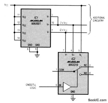
By adding a single component to a 3-V only or 5-V only board,you can operate conventional CMOS analog switches with Performance approaching that specified with ±15-V Supplies, This means fast switching,low ON resistance,CMOS /TTL compatibility, low power consumption,and a signal range (±Vcc) that exceeds the input supply range (Vcc to ground).Simply add a charge-ump voltage converter:(IC1),which produces±2-Vcc outputs from a Vcc input .These unregulated voltages ensure reliable switch operation for Vcc levels as low as 3 V. Logic thresholds for the switch remain unaffected A Vcc of 3 V (for instance)produces,±6 v rails for the switch (IC2),resulting in ON resistance<30Ω,switching times<200 ns,leakage<0.1 nA,and Vcc ourrent<0.5mA Raising Vcc to 5 V produces±10-V rails,resulting in ON resistance<20Ω,switching times<150 ns,leakage<0.4 nA,and Vcc current<l.3 mA IC1 can easily power additional switches and/or low-power Op amps,but more than a few milliamperes of load current degrades Performance by lowering the unregulated supply rails.
(View)
View full Circuit Diagram | Comments | Reading(875)
CRT_CONTROL
Published:2009/7/15 21:34:00 Author:Jessie
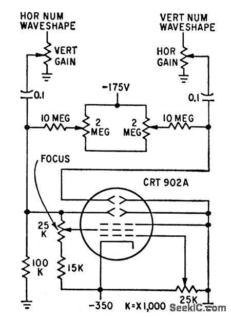
Takes waveforms from gates and applies them to deflection electrodes of 2-inch crt to create numeral-forming Lissajous patterns.-R. L. White, Forming Hand-written-Like Digits on CRT Display, Electronics, 32:11, p 138.140. (View)
View full Circuit Diagram | Comments | Reading(838)
STEPPER_MOTOR_SPEED_AND_DIRECTION_CONTROLLER
Published:2009/7/15 23:24:00 Author:Jessie
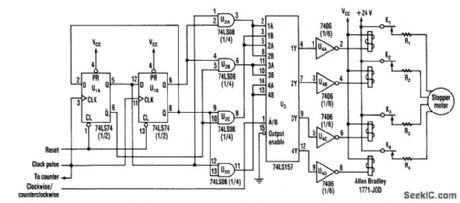
This new circuit uses four chips, with an option of using just three (the flip-flops and AND gates can be combined). The rate of clock pulses determines the motor's rpm. Switching transistors can replace the relays to increase the circuit's efficiency. This circuit drives a stepper motor whose speed depends on clock rate. Standard SS1 LSTTL chips are used. Switching transistors can be used in place of the solid-state relays to improve the circuit's efficiency. This new circuit uses four chips, with an option of using just three (the flip-flops and AND gates can be combined). The rate of clock pulses determines the motor's rpm. Switching transistors can replace the relays to increase the circuit's efficiency. This circuit drives a stepper motor whose speed depends on clock rate. Standard SS1 LSTTL chips are used. Switching transistors can be used in place of the solid-state relays to improve the circuit's efficiency. (View)
View full Circuit Diagram | Comments | Reading(1714)
ALARM_CONTROL
Published:2009/7/14 2:13:00 Author:May
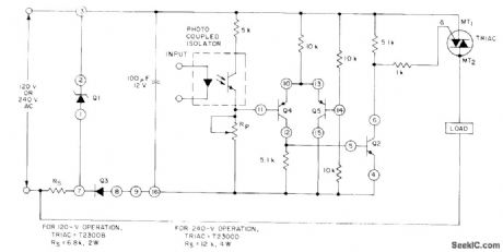
Any input suitable for driving LED of optoisolator triggers triac for energizing load such as alarm gong. Transistors Q4 and Q5 of CA3096 array serve as comparator. Diode-connected transistor Q3, zener-connected transistor Q1, and 100-μF capacitor develop DC supply voltages from AC line.- Circuit ideas for RCA Linear ICs, RCA Solid State Division, Somerville, NJ, 1977, p 9. (View)
View full Circuit Diagram | Comments | Reading(974)
PNP_SWITCHES
Published:2009/7/14 2:13:00 Author:May
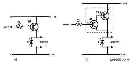
This figure shows two examples of a transistor PNP switch∶ (a)a single transistor and (b)a Darlington transistor. (View)
View full Circuit Diagram | Comments | Reading(1111)
SPDT_PIN_DIODE_HIGH_SOLATION_SWITCH_CIRCUIT
Published:2009/7/14 2:10:00 Author:May
This circuit is a basic SPDT PIN-diode switch using a series- and shunt-diode building block. Resistance R is chosen from Idiode =(Vcc-Vdiode)/R, where Idiode is the specified diode current and R is total dc circuit resistance. (View)
View full Circuit Diagram | Comments | Reading(851)
PIN_DIODE_HIGH_SOLATION_SWITCH_CIRCUIT
Published:2009/7/14 2:07:00 Author:May
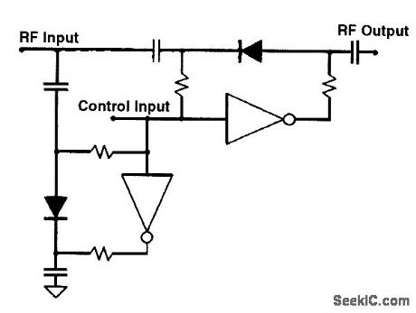
This circuit is a basic PIN-diode switch using series- and shunt-diode building blocks. R is chosen from Idiode=(Vcc-Vdiode)/R, where Idiode is the specified diode current and R is total dc circuit resistance. (View)
View full Circuit Diagram | Comments | Reading(836)
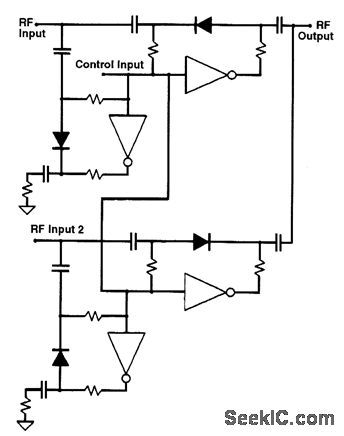
SERIES_SHUNT_PIN_DIODE_RF_SWITCH
Published:2009/7/14 2:03:00 Author:May
A combination of series and shunt switching results in superior isolation between the input and output when in the OFF condition. Diodes can be MV3404 or similar types. (View)
View full Circuit Diagram | Comments | Reading(0)
VHF_TRANSCEIVER_T_R_SWITCH
Published:2009/7/14 2:01:00 Author:May
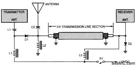
This is a transceiver transmit/receive switch that uses a PIN diode instead of a relay. Diodes can be MV3404 or similar types. (View)
View full Circuit Diagram | Comments | Reading(790)
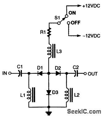
BASIC_PIN_DIODE_RF_SWITCH
Published:2009/7/14 1:59:00 Author:May
D1 is a pin diode (MV3404) used as a SWitch,with dc bias supplied via R1. L1 and L2 are RF chokes An alternative approach eliminating the RF chokes is also shown (View)
View full Circuit Diagram | Comments | Reading(1206)
4_A_FULL_WAVE_CONTROL
Published:2009/7/14 1:42:00 Author:May
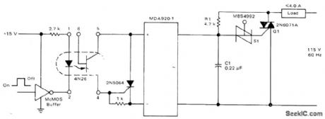
When logic input to CMOS buffer goes high, load is off. Low input logic deenergizes optoisolator; clamp formed by bridge rectifier and SCR is then removed from C1, allowing it to charge through R1. When voltage across C1 reaches triggering voltage of S1 (about 8 V), MBS4992 silicon bidirectional switch fires, allowing C1 to dump charge into gate of triac. Triac and load are then turned on.R1 and C1 are chosen to give time constant small enough to fire triac early in its conduction angle (near zero crossing), to maximize load power while minimizing EMI.-A. Pshaenich, Interface Techniques Between Industrial Logic and Power Devices, Motorola, Phoenix, AZ, 1975, AN-712A, p 17. (View)
View full Circuit Diagram | Comments | Reading(859)
ZERO_CROSSING_CONTROL
Published:2009/7/14 1:37:00 Author:May
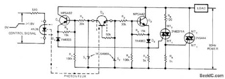
When control signal calls for power, optoisolator energizes circuit that provides load turn-on at zero-voltage time of AC waveform. If phototransistor Q3 of optoisolator is illuminated after S1 drops to 1-V conduction voltage of MUS4988, triacs will not be turned on. Circuit thus provides relay-enabling voltage window, lower limit of which is point at which all components involved in turning on triacs are forward-biased. Upper limit is nominal 8-V breakover voltage of unilateral switch S1. S2 performs similar function on negative voltage alternations. Load-controlling triac is rated 40 A.-T. Mazur, Solid-State Relays Offer New Solutions to Many Old Problems, EDN Magazine, Nov. 20, 1973, p 26-32. (View)
View full Circuit Diagram | Comments | Reading(1415)
400_CPS_FORK_CONTROL
Published:2009/7/15 22:35:00 Author:Jessie
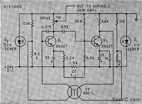
Tuning-fork oscillator gives frequency accuracy of 0.01% for d-c to a-c inverter. Consists essentially of two-stage amplifier, output of which is regeneratively coupled to input through tuning fork.-R. Wileman, Linear Circuits Regulate Solid-State Inverter, Electronics, 33:16, p 61-63. (View)
View full Circuit Diagram | Comments | Reading(927)
ANODE_TRIGGERED_RING_COUNTER
Published:2009/7/14 1:29:00 Author:May
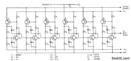
Triggered by coupling emitters of transistors Q1 to common bus, to permit both forward and reverse operation. Use of pnp-npn pairs reduces power requirements, improves load capacity, increases speed, and simplifiers circuits.-N. C. Hekimian, PNP-NPN CIRCUITS: New Look at a Familiar Connection, Electronics, 35.47, p 42-46. (View)
View full Circuit Diagram | Comments | Reading(2021)
VOICE_ACTIVATED_TAPE_RECORDER_SWITCH
Published:2009/7/14 1:27:00 Author:May
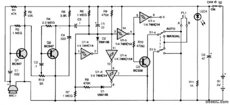
A schematic of the tape recorder switch is shown The circuit can be powered by B1, which is four AA batteries in series or any 6-Vdc supply. Audio signals from the electret Microphone,MIC1,are coupled via capacitor C1 to two audio-amplification stages centered around transistors Q1 and Q2 A 5000-Ω Potentiometer, R12,provides a sensitivity control that sets the audio level at which the switch will activate a tape recorder The audio input to the digital switching section of the circuit is biased at half the supply voltage by two 1-percent,1-MΩ,metal-film resistors (R6 and R7) Integrated Circuit U1 is a 74HC14 hex Schmitt-trigger inverter. With a 6-V power supply,the Schmitt inverter gates will have a l-V hysteresis gap between 2.2 and 3.2 V That means that the input to a Schmitt inverter must rise above 3.2V for the output to go low; but must fall below 2.2V for the output to return to a high,The low on pin 3 of U1-b in the Presence of audio is presented to pin 11 of U1-e and ends up at pin 8 of U1-d That will pull pin 1 low in the absence of an audio signal from the microphone,making pin 2 high Diode D2 blocks the discharging of C5 through its original charging path, so C5 starts to discharge through R9. After that delay, the voltage at pin 3 rises above 3.2 V, thus removing the connection from terminal A to ground and turning off the tape recorder. A continuous audio input to pin 1 will hold pin 4 high, but soon as it ceases, the time-out process begins. When power is applied to the circuit using switch S2, LED1 lights. However, if the ground connection to R11 is removed, and that end of the resistor is then connected to terminal X (pin 6 of U1-c), the LED will instead light only when the output of the circuit is active. (View)
View full Circuit Diagram | Comments | Reading(1674)
GROUND_REFERENCED_RAMP_AND_PEDESTAL_CONTROL
Published:2009/7/14 1:08:00 Author:May
Need for transformer is eliminated by applying alternate half-cycles to inverting and noninverting inputs of section 3 of LM3900 quad opamp, so full-wave-rectified waveform is referenced to ground. Comparator opamp 1 discharges timing capacitor at zero line voltage and synchronizes circuit with line frequency. Buffer opamp 2 scales input and provides linear pedestal for capacitor. Opamp 4 is comparator serving as output driver whose output is high when capacitor is charged to level selected by high-end trimming pot. Output is sufficient for optoisolators and logic triacs.-J.C. Johnson, Ramp-And-Pedestal Phase Control Uses Quad Op Amp, EDN Magazine, June 5, 1977, p 208 and 211. (View)
View full Circuit Diagram | Comments | Reading(1179)
80_VRMS_ANALOG_SWITCH
Published:2009/7/14 1:07:00 Author:May
Developed for switching high-level analog signals with speed, accuracy, and reliability, for such applications as digital-to-synchro converters. Feedback net-work stabilizes output against changes in circuit parameters. For AC signal inputs between±10 V, -12 VDC on gate of FET blocks input channel and R2 grounds inverting input of opamp A1 to prevent noise pickup and minimize voltage offset. Grounding gate of FET turns on input channel;input signal is then amplified by A1 and fed to unity-gain power opamp A2.-D.J. Musto, Analog Switch and IC Amp Controls 80V RMS, EDN Magazine, Feb 20, 1973, p 91-92. (View)
View full Circuit Diagram | Comments | Reading(1015)
DUAL_FUNCTION_SWITCH
Published:2009/7/14 1:05:00 Author:May
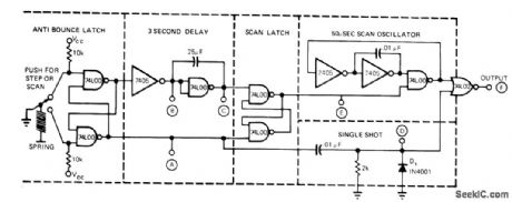
Pressing switch for less than 3 s produces single output pulse about 5μs wide. When switch is pressed longer than 3 s, single pulse is generated as before, and scan oscillator is turned on 3 s later. Oscillator runs as long as switch is held down, for producing repetitive stepping motion. Applications include positioning of test probes on single semiconductor chip or on wafer of several hundred chips, or indexing device either step by step or automatically through desired number of steps.-J. McDowell, Single Switch Controls Two Functions, EDN Magazine, April 5, 1974, p 78 and 80. (View)
View full Circuit Diagram | Comments | Reading(872)
| Pages:99/312 At 2081828384858687888990919293949596979899100Under 20 |
Circuit Categories
power supply circuit
Amplifier Circuit
Basic Circuit
LED and Light Circuit
Sensor Circuit
Signal Processing
Electrical Equipment Circuit
Control Circuit
Remote Control Circuit
A/D-D/A Converter Circuit
Audio Circuit
Measuring and Test Circuit
Communication Circuit
Computer-Related Circuit
555 Circuit
Automotive Circuit
Repairing Circuit