
Electrical Equipment Circuit
Index 18
The white light LED driver circuit of high current
Published:2011/8/11 22:16:00 Author:Borg | Keyword: white light, LED driver, high current
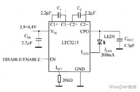

The white light LED driver circuit of high current can be formed by LTC3215, and its output current of the drive white light LED is 700mA. It can switch automatically among the voltage-multiplying types of 1, 1.5 and 2 times, which can make LTC3215 get a high efficiency of 92% in the whole working voltage range of the lithium ion battery. The typical application circuit of LTC3215 is shown in figure 1 and its efficiency curve is shown in figure 2.
Figure 1 The typical application circuit of LTC3215
Figure 2 the efficiency curve of LTC3215 (View)
View full Circuit Diagram | Comments | Reading(1235)
TL431 Basic Application Circuit
Published:2011/8/11 23:23:00 Author:Robert | Keyword: Basic, Application
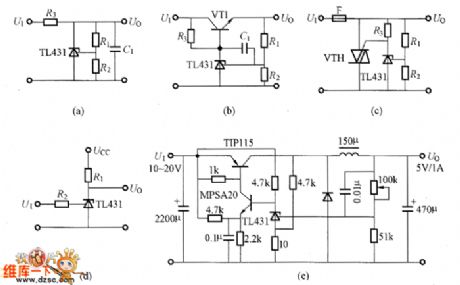
The TL431 basic application circuit is shown in the picture.
(a)Parallel voltage regulator circuit. (b)Series voltage regulator circuit. (c)Over-voltage protection circuit by using VTH. (d)Convertor with wide temperature compensationvalue. (e)Voltage regulator power with output 5V/1A. (View)
View full Circuit Diagram | Comments | Reading(8849)
ICBT Grid Electrode Driving Control Power Circuit
Published:2011/8/16 10:35:00 Author: | Keyword: ICBT, Grid Electrode, Driving, Control, Power

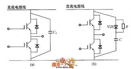
The ICBT grid driving circuit itself is using the hybrid method. Its internal optocoupler type, high-voltage type IC would make it small. But the control power, which provide power for the grid electrode driving circuit, should use the transformer and smoothing capacitor and so on. For the driving circuit overall miniaturization, it should consider the miniaturization of these elements. So it would take different ways for the control circuit, which are shown in the picture. The picture (a) is transformer method. It is a stable power of which the high and low side IGBT can get the same voltage. The picture (b) is the bootstrap method. The C1 is the bootstrap capacitance. The VD1 should select the high-voltage diode. The inverter's output duty cycle shouldn't be 100%. (View)
View full Circuit Diagram | Comments | Reading(1647)
IGBT Grid Electrode Driving Circuit
Published:2011/8/13 7:03:00 Author:Robert | Keyword: IGBT, Grid Electrode, Driving
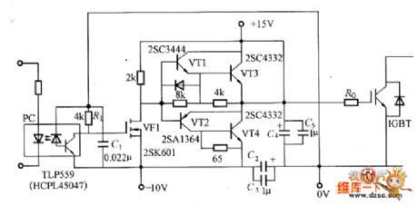
The picture shows the IGBT grid electrode driving circuit practical example. This circuit should be noted the following tips:(1)PC should choose the optical coupler which has fast response speed and strong ability to remove the common-mode noise, such as HCP4504, TLP559 and so on.(2)It should take measures to aviod the optical coupler's error action caused by the driving power variation. For example, the R1 and C1 can make up the anti-interference circuit.(3)The C2 and C4 are the smoothing capacitances used for the driving power. Its capacitance value is chosen to be 100 times of Cies (Cies is the input capacitance of the IGBT). The C3 and C6 are in parallel with the C2 and C4 which should have the good high-frequency features. They are used to filter the high-frequency noise. (View)
View full Circuit Diagram | Comments | Reading(3322)
IGBT Absorbing Circuit
Published:2011/8/16 10:13:00 Author: | Keyword: IGBT, Absorbing
Except the large-capacity devices, the IGBT absorbing circuit has two kinds which are shown in the picture. And, the picture (a) is the most simple capacitance absorbing circuit (C absorbing circuit). The main circuit's inductor and capacitor C1 would generate the resonance. If C1 is too small or the main circuit inductor is too large, the DC power wire's voltage would have a big variation. The picture (b) shows the resistance-capacitance diode absorbing circuit (RCD absorbing circuit) which is complex. But the DC power wire's voltage has small variation. When the main circuit inductor is big, this absorbing circuit's performance of limiting the surge voltage would be good. But it should note the function of diode VD1. If having wrong selection it would generate the voltage oscillation. (View)
View full Circuit Diagram | Comments | Reading(1216)
IGBT Driving Circuit Composed Of EXB840
Published:2011/8/11 6:44:00 Author:Robert | Keyword: IGBT, Driving
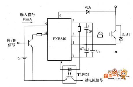

The IGBT driving circuit composed of EXB840 is shown in the picture. (View)
View full Circuit Diagram | Comments | Reading(1626)
Grid Electrode Drivng Circuit Composed Of M57918L
Published:2011/8/17 0:30:00 Author: | Keyword: Grid, Electrode, Drivng
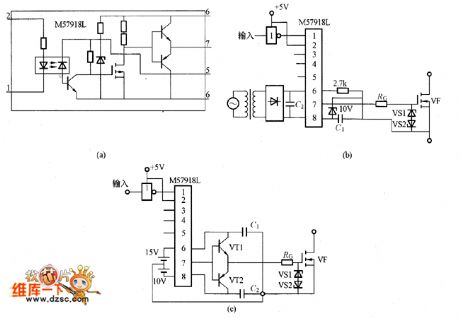
The picture shows the the grid electrode driving circuit composed of M57918L. The picture (a) is the M57918L internal equivalent circuit. The picture (b) shows the circuit driving the low-power MOSFET. In the circuit the C1 and C2's capacity is more than 200 times than Ciss (the input capacitanc of the MOSFET). If using the electrolytic capacitor, it needs to add the film capacitor in parallel with electrolytic capacitor and the film capacitor should have good high-frequency features. Its capacity is 1/200 of the C1 or C2's capacitor. The lower of the RG, the higher the switching speed would be, but it shouldn't be lower than its lower limit. The VS1 and VS2 need the regulator diode about 18V. The picture (c) is the circuit which is driving the large-power MOSFET. (View)
View full Circuit Diagram | Comments | Reading(1240)
Grid Electrode Driving Circuit Composed Of IR2121
Published:2011/8/17 9:45:00 Author: | Keyword: Grid, Electrode, Driving
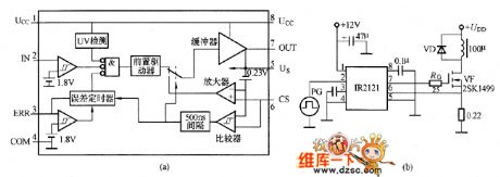
The picture shows the grid electrode driving circuit composed of IR2121. The IR2121 is a low-side grid electrode driving IC with the current-limiting function. The picture (a) shows the IR2121 internal equivalent circuit. The IR2121 has the error output port (ERR). The circuit shut-off time is set by the ERR port with the external connected capacitor. The input (IN) signal voltage level is TTL positive logic level. The threshold voltage is 1.8V. The power detecting port (CS) threshold voltage is 230mV with internal setting 500ms interval. The delay time's typical value is 700ns from detecting the over current to the circuit shutting off. (View)
View full Circuit Diagram | Comments | Reading(4180)
Grid Electrode Driving Circuit Composed Of TK75050
Published:2011/8/17 9:46:00 Author: | Keyword: Grid, Electrode, Driving

The picture shows the grid electrode driving circuit composed of TK75050. The TK75050 has the internal functions such as current limiting, thermal breakdown protection, low voltage lockout and so on. The load capacitance is 10000pF. It is the low-side grid electrode driving IC with in or out current of ±2A. The picture (a) shows the TK75050's internal equivalent circuit. And when the internal temperature is about 150℃ the over-heat protection circuit would have action. Its input (INPUT) threshold voltage is 1.6V/1.0V which is the so-called TTL voltage level. Its working voltage Ucc is 12V and if it is under 11V the low-voltage lockout circuit would have action, if it is under 10V the circuit would be shut off. This is prevent the unstable working of the circuit when its power voltage varies slowly. (View)
View full Circuit Diagram | Comments | Reading(1130)
Low-Voltage Port (Shortly Called Low Port) Grid Electrode Driving Circuit
Published:2011/8/17 0:18:00 Author: | Keyword: Low, Voltage, Port, Grid Electrode, Driving
(View)
View full Circuit Diagram | Comments | Reading(988)
Grid Electrode Driving Circuit Composed Of Two Transistors
Published:2011/8/16 23:38:00 Author: | Keyword: Grid, Electrode, Driving, Two, Transistors
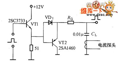
The picture shows the grid electrode driving circuit composed of VT1 and VT2 which are in the emitter follower working mode. For the power MOSFET whose drain electrode's power consumption of 100~150W, its input capacitance Ciss is thousands of pF. When the voltage UDS between drain electrode and source electrode is closing 0V, the input capacitance would increase and be more. So as the loading capacitance of the grid electrode driving circuit, the C1 is normally be 10000pF (about 0.01uF). The picture shows the grid electrode driving circuit. When the transistor VT1 is conducted it would charge the capacitor CL. When the transistor VT2 is conducted it would discharge the electricity stored by the grid electrode. The RG would limit the peak current of the charging and discharging. (View)
View full Circuit Diagram | Comments | Reading(1119)
XC62AP Series Integrated Voltage Regulator Internal Diagram And Basic Application Circuit
Published:2011/8/17 10:12:00 Author: | Keyword: Integrated, Voltage, Regulator, Internal, Diagram, Basic, Application
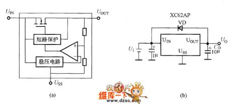
The XC62AP series integrated voltage regulator is a CMOS integrated voltage regulator with linear positive voltage output. It has output voltage of +5V (XC62AP50) and+3V (XC62AP30) and other types, which could arbitrarily set the voltage between 1.1V to 6.0V by the factory (stepped voltage is 0.1V). The XC62AP series integrated voltage regulator's internal diagram and basic application circuit is shown in the picture.
Picture (a) shows the XC62AP series integrated voltage regulator's internal diagram. Picture (b) shows the basic application circuit.
The picture shows the XC62AP series integrated voltage regulator's internal diagram and basic application circuit.
The XC62AP series integrated voltage regulator's features are super-low current consumption which typical value is 0.9uA, low voltage drop which has the typical value of 180mV at output current of 80mA, low deviation of output voltage which is about ±2%, small temperature drift. So it would be used as the super-low power consumption referenced voltage source. (View)
View full Circuit Diagram | Comments | Reading(1687)
RX5RA/RE Series Integrated Voltage Regulator Pin Configuration And Basic Application Circuit
Published:2011/8/14 5:53:00 Author:Robert | Keyword: Integrated, Voltage, Regulator, Pin, Configuration, Basic, Application

The RX5RA/RE series are three-port CMOS integrated voltage regulator with low voltage drop and low current consumption. The series have T092 and surface-mount package types. Their model names are different as their package. The T092 package is for RE5RA/RE and the surface-mount package is for RH5RA/RE. The picture shows the RX5RA/RE series integrated voltage regulator pin configuration and basic application circuit.
(a)RX5RA/RE series integrated voltage regulator pin configuration. (b)Basic application circuit.
The picture shows the RX5RA/RE series integrated voltage regulator pin configuration and basic application circuit. (View)
View full Circuit Diagram | Comments | Reading(1038)
RN5RG Series Voltage Regulator Internal Diagram And Basic Application Circuit
Published:2011/8/18 2:22:00 Author: | Keyword: Voltage, Regulator, Internal, Diagram, Basic, Application

The RN5RC series is the low-voltage-drop voltage regulator with surface-mount small SOT23 package and externally connecting with a PNP transistor. The RN5RG30A (output voltage is 3V) features is following: no-load current consumption is 50pA, standby current is 0.2uA, input/output voltage difference is the transistor's conducted resistance value multiply by the output current. Its output voltage's accuracy is ±2.5%. Its output voltage's temperature feature is in ±100×10-6℃. Its input stability is 0.1%/V. It uses the SOT23 5-pin package.
The picture shows the RN5RG series voltage regulator internal diagram and basic application circuit. (View)
View full Circuit Diagram | Comments | Reading(1253)
LM2931 Basic Application Circuit
Published:2011/8/13 8:52:00 Author:Robert | Keyword: Basic, Application
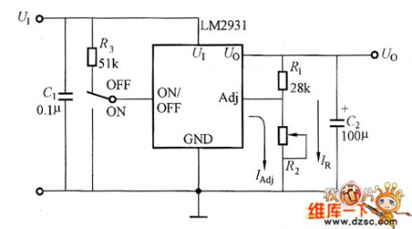
The voltage-adjustable LM2931 is a five-port voltage regulator. It adds the adjustment port (Adj) and on/off port. Its output voltage Uo is set by the resistor R1 and R2 which are connected to the Adj port. The LM2931 basic application circuit is shown in the picture. In the circuit internal part it should control the voltage between Uo-Adj ports to be the same to its internal referenced voltage Uref. (View)
View full Circuit Diagram | Comments | Reading(2495)
Three-Port Voltage Regulator Basic Application Circuit
Published:2011/8/18 6:56:00 Author: | Keyword: Three, Port, Regulator, Basic, Application
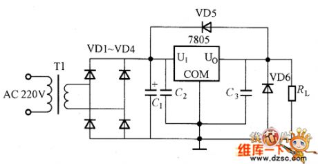
The picture shows the three-port voltage regulator basic application circuit (for example of 7805). The input AC 220V voltage would be through the transformer T1 for voltage buck and the VD1~VD4 bridge rectifier and smoothing capacitance C. After filtering it would get a very stable DC 8~12V voltage and add it to the 7805's input port. For making the circuit stably work, it is connected the capacitace C2, C1 and C3 at the input port and output port. The C2 is the input stability capacitance. When the regulator input impedance is reduced, for avoiding the oscillation, it could use the 0.1uF~1uF ceramic or tantalum capacitors. The C1 is the smoothing capacitance. If it is closing to the 7805, the capacitor C1 can be removed. (View)
View full Circuit Diagram | Comments | Reading(1243)
Three-Port Voltage Regulator Internal Equivalent Circuit
Published:2011/8/14 6:15:00 Author:Robert | Keyword: Three-Port, Voltage, Regulator, Internal, Equivalent
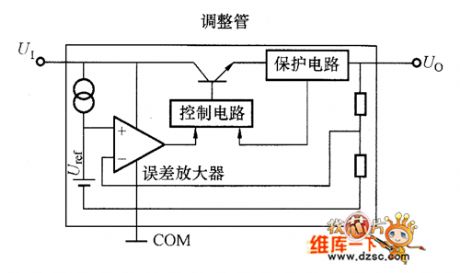
The three-port voltage regulator's three ports are input port U1, output port Uo and common port COM which is usually connecting to the ground. Its internal equivalent circuit is shown in the picture. It is made up by the adjustable tube, protection circuit, control circuit, error amplifier and so on. The voltage between Uo and COM port is comparing with the referenced voltage Uref. They are usually keeping same when working. And when the input voltage UI or output curent Io have variation, they would keep the output voltage Uo stable. (View)
View full Circuit Diagram | Comments | Reading(1123)
Regulator Power Circuit With Output Of 6V/5A
Published:2011/8/14 6:32:00 Author:Robert | Keyword: Power, Regulator, Output
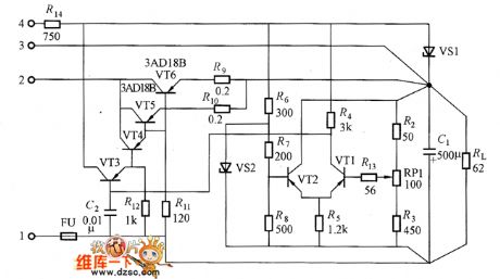
The picture shows the regulator power with output of 6V/5A. The adjustable tube is made up of VT3, VT4, VT5 and VT6. The VT5 and VT6 are in parallel to increase the output current. The R9 and R10 are current equalization resistors to reduce the effects of the differences of tube features and the ICBO. Generally the voltage drop on the resistor is 0.1~1V. (View)
View full Circuit Diagram | Comments | Reading(1347)
Regulator Power Circuit Which Using Transistor As Amplifier
Published:2011/8/13 9:09:00 Author:Robert | Keyword: Regulator, Power, Transistor, Amplifier

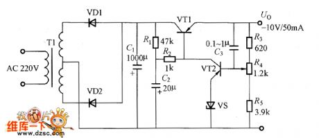
The picture shows the simple and practical regulator power with output voltage of -10V and output current of 50mA. The C2 is coupling capacitor. It makes the output port's ripple directly couple to the amplifier tube VT2's base electrode and it would not be through the sampling resistor. So the output voltage's ripple is very small. The C3 is selected between 0.1uF to 1uF. (View)
View full Circuit Diagram | Comments | Reading(1123)
Simple Transistor Regulator Power Circuit
Published:2011/8/14 6:42:00 Author:Robert | Keyword: Simple, Transistor, Regulator, Power
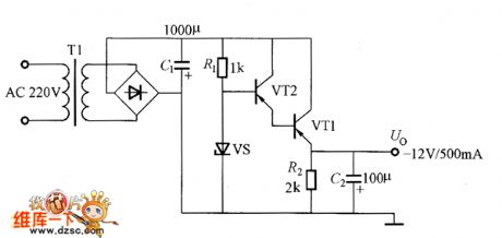
The picture shows the simple transistor regulator power circuit with output voltage of -12V and output current of 500mA. The adjustable tube VT1 and VT2 use the Darlington connecting method to improve the adjustment sensitivity. The C2's function is to further reduce the probable ripple. This circuit's output voltage is closing to the zener diode VS's reverse breakdown voltage, so it can't be adjusted. It is suitable for the cases which need large current and not very high stability. (View)
View full Circuit Diagram | Comments | Reading(1617)
| Pages:18/126 1234567891011121314151617181920Under 20 |
Circuit Categories
power supply circuit
Amplifier Circuit
Basic Circuit
LED and Light Circuit
Sensor Circuit
Signal Processing
Electrical Equipment Circuit
Control Circuit
Remote Control Circuit
A/D-D/A Converter Circuit
Audio Circuit
Measuring and Test Circuit
Communication Circuit
Computer-Related Circuit
555 Circuit
Automotive Circuit
Repairing Circuit