
Electrical Equipment Circuit
Index 21
On-Hook Anti Toll Fraud Device Circuit Diagram
Published:2011/8/9 18:26:00 Author:Vicky | Keyword: On-Hook, Anti Toll Fraud
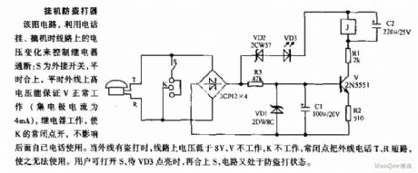
On-Hook Anti-Toll-Fraud Device
The circuit controls the on-off of relay by making use of the changes of voltage brought by on-hook and off-hook of the telephone. S is a exterior switch, which is closed usually. Usually the high voltage of the external line can guarantee the regular work of V (the current of collector is 4mA). The relay works, and the closed contact of K is open, which does not affect the usage of the telephone. When there is toll fraud in the external line, the voltage of the line is lower than 8V, K does not work, and the closed contact makes the external telephone T and R under short circuit. Therefore the external telephone T and R cannot work then. The user can open S, and close it after VD3 is lighted. Then the circuit is under anti-toll-fraud situation. (View)
View full Circuit Diagram | Comments | Reading(1501)
Telephone on-hook warning circuit diagram
Published:2011/8/9 18:31:00 Author:Vicky | Keyword: Telephone on-hook warning circuit
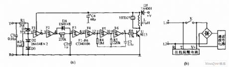
Telephone on-hook warning circuit diagram is shown in the above picture. The IC uses CMOS Shmidt hex inverter CD40106. C1 is better to use ceramic capacitance which can withstand voltage of over 100V, and L is better to choose small color-code inductor. There are no special requirements for the rest component. When the telephone is on-hook, there are several tens of volt-ampere in ends T and R. A short period of sound indicating on-hook is given out via HTD. It is shown in the picture (a). Because the sound only uses the memory function of C4, C4 can only be re-charged when the telephone is off-hook next time after the sound is given out. And the warning sound can be given out when the telephone is on-hook next time. The assembling diagram is shown in the picture (b).
(View)
View full Circuit Diagram | Comments | Reading(2110)
Simple telephone time lock circuit diagram
Published:2011/8/9 18:33:00 Author:Vicky | Keyword: Simple telephone time lock circuit
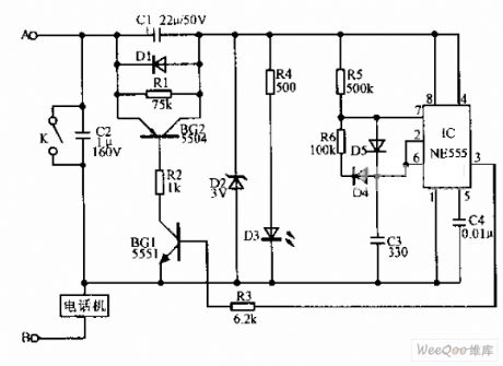
Simple telephone time lock circuit is shown in the above picture. In the circuit diagram, BG1 and BG2 are electronic switches controlled by IC NE555. When the telephone is on-hook, the DC resistance value of the telephone is over 600KΩ, the current when the external line runs into the IC is very low, and the electronic time lock does not work. When the telephone is off-hook, the telephone DC resistance value reduces to 500Ω, and the electronic time lock works. After the call has been made for a certain period of time, pin 3 of the IC turns into low potential, which forces BG1 to stop. The exterior pressure drop is mainly on the electronic switch, which results in the telephone’s inability to work. And the call is suspended. (View)
View full Circuit Diagram | Comments | Reading(2713)
Telephone Automatic Answering Device Circuit Diagram
Published:2011/8/9 18:34:00 Author:Vicky | Keyword: Telephone, Automatic Answering Device
Telephone automatic answering device circuit is shown in the above picture. The recording telephone device has strong ability of anti-disturbance, which avoids some unexpected matters. When the telephone rings for 6 times without answering, the device will imitate automatic off-hook. Then the telephone is on and gives out the following words: “hello, the host is not in home. Please leave a short message.” Meanwhile, the recorder is connected, and records the detailed content of the speaker’s words. (View)
View full Circuit Diagram | Comments | Reading(3184)
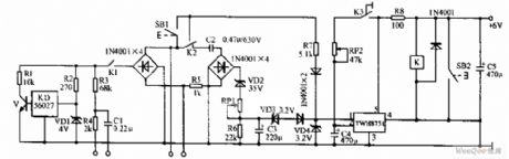
Telephone Automatic Recording Control Device Circuit Diagram
Published:2011/8/9 18:35:00 Author:Vicky | Keyword: Telephone, Automatic Recording Control Device
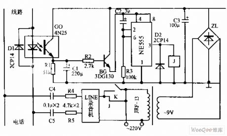
The telephone automatic recording control device circuit is shown in the above picture. When there is ringing signal in the line (90V, 15Hz) or the telephone is off-hook, the delayed pin 3 of NE555 shows high potential, which makes J conducted. The AC power supply of the recorder is conducted by the contact and automatically records the message. It stops recording when the telephone is off-hook or the power supply is cut. K is the manual-operational switch, and is used to control the power supply during sound reproduction. (View)
View full Circuit Diagram | Comments | Reading(1925)
Real-time Telephone Automatic Recording Device Circuit Diagram
Published:2011/8/9 18:38:00 Author:Vicky | Keyword: Real-time Telephone Automatic Recording Device
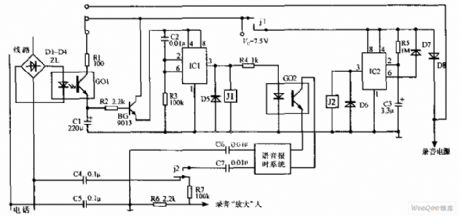
Real-time telephone automatic recording device circuit is shown in the above picture. Despite automatic recording for the making calls and answering calls, the recording device can also automatically input the time of recording before recording the message , which makes the recording material more detailed and accurate and thus easy to be picked out and analysis. IC1 and IC2 in the picture are time-base integrated circuit NE555. The voice timing system uses UT-6657 type made-up timing table. Relay J1 and J2 are HG4098. The coupling device is 4N15, and the diodes are IN4007. (View)
View full Circuit Diagram | Comments | Reading(1946)
Microcomputer Telephone Cost-Saving Device Circuit Diagram
Published:2011/8/9 18:40:00 Author:Vicky | Keyword: Microcomputer Telephone Cost-Saving Device
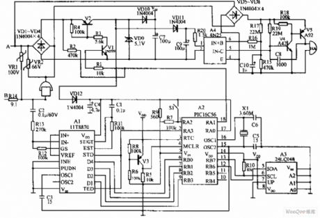
The microcomputer telephone cost-saving device circuit is shown in the above picture. The circuit is made of anti-wiretapping and central processing. PIC16C56 is the central part of the whole circuit. Anti-wiretapping part is composed by VD5-VD8, A4, V4, V5 and HA. The operation of the device is very simple. It has no limitation on the business phones and the phones can be dialed directly; when making business calls, dial the general code first and then dial the telephone number. Then hang up the phone for 4S. The device automatically goes back to the state of limiting the non-business telephone. (View)
View full Circuit Diagram | Comments | Reading(2572)
Circuit Diagram of adding visual judgment function to telephone ringing
Published:2011/8/9 18:18:00 Author:Vicky | Keyword: visual judgment function , telephone ringing
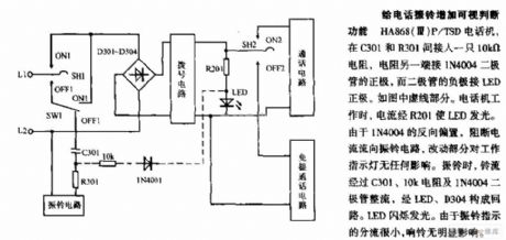
HA868(Ⅲ) P/ TSD telephone, adds a resistance of 10K Ω indirectly between C301 and R301, and connects the anode of diode IN4004 with the other side of the resistance while connects the cathode of the diode with the anode of LED. It is shown by dotted line in the picture. When the telephone works, the current goes through R201 and make the LED lighted. Because IN4004 is reversely biased, and prevents the current from flowing to ringing circuit, the revised part has no affection towards working indication light. When it starts ringing, the ring flows through C301, resistance of 10KΩ and diode IN4004, and becomes a loop via LED and D304. LED then twinkles and gives out light. Since the shunt of the ringing indication is very small, the ring is obviously affected. (View)
View full Circuit Diagram | Comments | Reading(1436)
Ring current generator circuit diagram
Published:2011/8/9 18:20:00 Author:Vicky | Keyword: ring, current generator
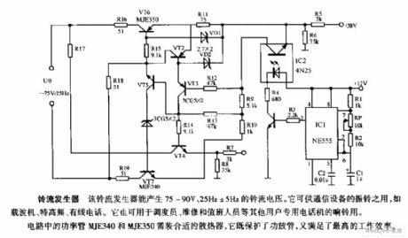
Ring current generator
The ring current generator can produce a ringing current voltage of 75-90V and 25Hz±5HZ. It is available to be used for vibrating ring in communication devices, for example, carrier, ultrahigh frequency, wire telephone. It can also be used as ring in special telephone for dispatchers, repairmen, operators on duty and other users.
The power tube MJ3340 and MJE 350 in the circuit need suitable radiator to protect the power amplification tube and improve the work efficiency. (View)
View full Circuit Diagram | Comments | Reading(4735)
Circuit diagram of auto-adjustment for the telephone ring
Published:2011/8/9 18:22:00 Author:Vicky | Keyword: auto-adjustment , telephone ring
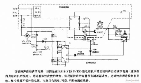
Auto-adjustment circuit of the telephone ring
The above picture is the auto-adjustment circuit added into the HA18(ⅤⅡ) P/ TSD type telephone (the circuit within the dotted frame is the original circuit of the telephone.). With the increasing numbers of the ring times, the gradual change of the ring volume and tone can be achieved and also the goal of control thr ringing procedure can be reached. The whole device needs no peripheral power supply. The circuit is simple and reliable. In addition , it does not affect the communication line. (View)
View full Circuit Diagram | Comments | Reading(1395)
Circuit diagram of constant-current-source type power supply and off-hook detection
Published:2011/8/9 18:23:00 Author:Vicky | Keyword: constant-current-source , power supply , off-hook detection
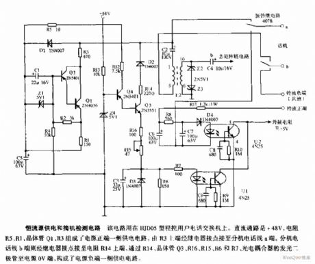
Circuit diagram of constant-current-source type power supply and off-hook detection
The circuit is used for HJD05 –type switching board. The direct current path is + 48V, and the resistances R5, R1, and the transistors Q1, Q3 constitutes a supply circuit in the positive end of the power supply. The upper end of R3 is connected with a end of the extension’s telephone line via a relay. The b end of the extension’s telephone line is connected to upper end of resistance R14 via a relay. The b end then is connected with 0V end of the power supply via R14, transistors Q3, R16, R15, R5, and R7, and the luminous diodes of the photoelectric coupler, which constitute the supply circuit in the negative end of the power supply. (View)
View full Circuit Diagram | Comments | Reading(3363)
Light-Operated Ring Circuit Diagram
Published:2011/8/9 18:24:00 Author:Vicky | Keyword: Light-Operated Ring
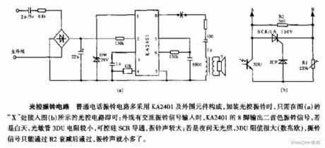
Light-Operated Ring Circuit
Average telephone ring circuit is composed of KA2401 and peripheral components. When adding light-operated ring circuit, just connects the part “X” in picture a with light-operated circuit in picture b. When there is input of AC ring signal into the exterior line, the pin 8 of KA2401 outputs ring signal of two tones. In the daytime, light sensitive tube 3DU has low resistance value, the SCR is conducted, and the volume of ring is relatively higher; in the evening, when there is no light, the resistance value of 3DU is very high (several megohms), the ring signal is weakened by R2 before passing through , so the volume of ring is much lower. (View)
View full Circuit Diagram | Comments | Reading(2059)
FM Wireless Microphone Circuit Diagram
Published:2011/8/9 18:01:00 Author:Vicky | Keyword: FM , Wireless Microphone
The following measures are taken to promise a clear voice of the microphone: the output signal of MIC is first sent to BG1 to be amplified. R1 and C1 is the additional pre-emphasized high-pitch sound circuit. C2 and C3 is the input and output coupling capacitance of tube BG1, the value of which is relatively lower to reduce the low-pitch sound and raise the mid and high sound. The diodes D3 and D4, which is connected in parallel in the BG1 output end , and the circuits C4 and C7, make use of the feature of the internal resistance ‘s being lower when the diodes are conducted in forward direction and influence the strong signal by limiting the amplitude. However, the regular signals remains unaffected. (View)
View full Circuit Diagram | Comments | Reading(3429)
Sanhe Brand Anti-Theft Door Talkback Doorbell Analysis Circuit
Published:2011/8/7 21:54:00 Author:Robert | Keyword: Sanhe, Anti-Theft, Door, Talkback, Doorbell, Analysis
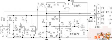
The corridor anti-theft door is the public protection facilities of the urban families. Its talkback doorbell would offen have faults in house decoration and normal using. This article introduces the Sanhe brand SH25 type anti-theft door talkback doorbell (indoor device) working principle which would be reference for maintaining this device and other equivalent products. The circuit is shown in the picture (in the picture the voltage marked with CN1 is the practically tested voltage when open circuit).1.Visitors pressing the button to call the master. When the visitors press the corresponding room number's doorbell switch, the CN1's pin 3 would send DC voltage to supply the working voltage for the IC1 through R11 for voltage divider. And the voltage would be bucked through R5 that indicates the working mode by Z3. Also it is changed to be 3V voltage as the working power of the musical chip IC2 (KD-9300A) through R8's voltage step-down and Z1's voltage regulator. At the same time the C8 would complete the triggering. The IC2 would generate the doorbell's calling signal and then send to the tone amplifier IC1 (LM386) for amplification. And then it would output from the pin 5 and is send to the headphone for sounding through the key switch, C4, RW2. Thus it completes the doorbell calling. (View)
View full Circuit Diagram | Comments | Reading(1439)
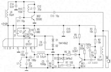
Mobile Phone Sensor-900mhz RF Indicator Circuit
Published:2011/8/7 21:53:00 Author:Robert | Keyword: Mobile Phone Sensor-900mhz RF Indicator Circuit
When the mobile phone is in the standby mode and receives the calling signal from the base station, it would transmitter the answer signal. So that the mobile phone's antenna would also have a short time while the RF signal is sending. At this time, is there is a micro sensor beside the mobile phone, it would flash the red light. Some other kinds of sensors could also have the music. By the analysis of the sensor circuit, it is found that it is practically a 900MHz RF indicator. Here the analysis of its working principle is introduced.The 900MHz RF indicator's principle circuit is shown in the picture. The RF signal is received by the spring steel wire L1 which is used as the antenna (w) (L2 is a current-limiting coil with only one cycle). The signal then is sended to VT1 for amplification through C1. The VT1 is in the critical conduction mode at the functions of bias resistor R1 and R2. When no signal the VT1's collector polar is in high voltage level to make the PNP tube VT2 closed. So the multivibrator would not work which is made up of VT3 and VT4. (View)
View full Circuit Diagram | Comments | Reading(2614)
Sound Control Toy Kitten Circuit
Published:2011/8/7 21:53:00 Author:Robert | Keyword: Sound, Control, Toy, Kitten
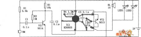
The sound control toy kitten circuit is shown in the picture. It is made up of two parts which are sound control switch and kitten mew generator. The microphone BM is a sound wave receiver. When it receives the applause sound wave signal, it would output corresponding electric signal to the transistor VT1's base polar for amplification through the capacitor C1. After amplification the signal would output from the VT1's collector polar and be added on the kitten mew IC KD-5605's trigger port through the capacitor C2. Then it would trigger the IC to work. The IC would outpout three times of kitten mew sound which would be amplified by the transistor VT2 and then impulse the small electromagnetic buzzer BL to sound. And also it would drive two LEDs (LED1, LED2) to have the synchronized flash with the kitten mew sound. (View)
View full Circuit Diagram | Comments | Reading(1882)
Flashing Musical Gyroscope Circuit
Published:2011/8/7 21:53:00 Author:Robert | Keyword: Flashing, Musical, Gyroscope
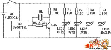
The picture shows the flashing musical gyroscopic circuit. It is made up of musical IC UM66T19L and multi-color LED LED1~LED4. When the gyro is in the rotation mode, because of the function of centrifugal force, the centrifugal switch S1 is connected and the power is added on the four LED directly to make they light. Also the IC1 is connected to the power, the buzzer BL would sound the music. The centrifugal switch S could be self-made by using the elastic metal sheet. It needs to be adjusted for many times and thus it could get a good performance. Also the gyro is a rotated moving object, its overall balance is very important. So the PCB's layout should not only be left-and-right symmetrical, but also should consider the weight balance in the vertical direction. (View)
View full Circuit Diagram | Comments | Reading(2205)
Ultrasonic Liquid Level Indicator Circuit Composed Of NE555
Published:2011/8/7 21:57:00 Author:Robert | Keyword: Ultrasonic, Liquid Level, Indicator
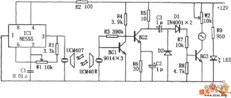
The picture shows the ultrasonic liquid level indicator circuit. This circuit is made up of ultrasonic transmitter circuit and receiver circuit.The ultrasonic transmitter circuit is made up of 555, R1, W1, C1 and ultrasonic transmitter head UCM40T. The ultrasonic receiver circuit is made up of the corresponding receiving head UCM40R, cascade amplifier BG1 and BG2, detecting circuit and so on. When the liquid level is closing to the receiver head, the voltage meter's deflection angle would be increasing. The closer to the liquid level, the bigger the corresponding deflection angle would be.Because the ultrasonic has the featrue that it would not be effected by the liquid's concentration and electric conductivity, so this circuit would be better and have higher accuracy than general contacting liquid level display circuit. (View)
View full Circuit Diagram | Comments | Reading(4948)
CXA-1213S Luminance And Chrominance Signal Processing Integrated Circuit
Published:2011/7/13 22:02:00 Author:Robert | Keyword: Luminance, Chrominance, Signal, Processing, Integrated
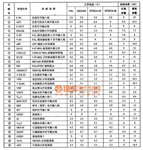
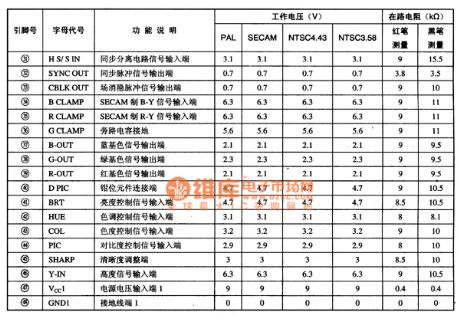
The CXA-1213S is a luminance and chrominance signal processing IC produced by the Sony company which is widely used in sony series large-screen color TV sets.
1.Its functional features.
The CXA-1213S IC has internal color format detection and conversion circuit, chrominance signal decoding circuit and its corresponding auxiliary circuit.
2.Its pin's function and data.
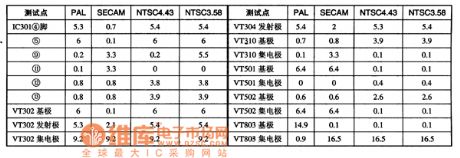
The CXA-1213S IC uses 48-pin dual inline package. Its pin's function and data is listed in table 1. The format conversion circuit key points' voltage is listed in table 2.
The table 1 shows the CXA-1213S IC's pin's function and data.
The table 2 shows the format conversion circuit key points' voltage.
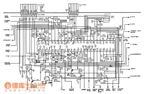
3.Typical application circuit.
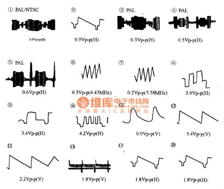
The CXA-1213S IC's typical application circuit is shown in picture 1. The CXA-1213S related pins' waveform is shown in picture 2. (This picture is the original picture of the color TV sets, so the symbols which don't meet the standard have not been modified).
The picture 1 shows the CXA-1213S IC's typical application circuit.
The picture 2 shows the CXA-1213S IC's related pins' signal waveform. (View)
View full Circuit Diagram | Comments | Reading(8455)
Logic Signal Long Time Delay Circuit
Published:2011/8/2 21:49:00 Author:Robert | Keyword: Logic, Signal, Long, Time Delay
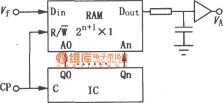
If you want to make the serial input logic signal Vtoutputafter thedelay time, it could use the circuit shown in the picture. This circuit uses a RAM and a binary counter. They could both use a same clock signal CP. In the first half cycle of the clock signal, the counter's data would add 1 which would output as the address for reading data. In the next half cycle of the clock signal the new input data Vf would be writen to the same unit. This signal could be read after the time of td=2n+1Tcp. Here Tcp is the cycle time of the clock signal. (View)
View full Circuit Diagram | Comments | Reading(1360)
| Pages:21/126 At 202122232425262728293031323334353637383940Under 20 |
Circuit Categories
power supply circuit
Amplifier Circuit
Basic Circuit
LED and Light Circuit
Sensor Circuit
Signal Processing
Electrical Equipment Circuit
Control Circuit
Remote Control Circuit
A/D-D/A Converter Circuit
Audio Circuit
Measuring and Test Circuit
Communication Circuit
Computer-Related Circuit
555 Circuit
Automotive Circuit
Repairing Circuit