
Electrical Equipment Circuit
Index 35
PRINT_TIMER
Published:2009/7/21 4:24:00 Author:Jessie

Uses radar phantastron circuit to give correct combination of exposure time and color filtier for desired contrast and density. R1 sets exposure time from 6 to 60 seconds and R2 regulates contrast.-J. D. Weir, Print Timer Controls Density and Contrast, Electronics, 31:7, p 108-109. (View)
View full Circuit Diagram | Comments | Reading(890)
Very_high_impedance_instrumentation_amplifier_using_two_AD510s_and_two_AD515s
Published:2009/7/21 3:12:00 Author:Jessie
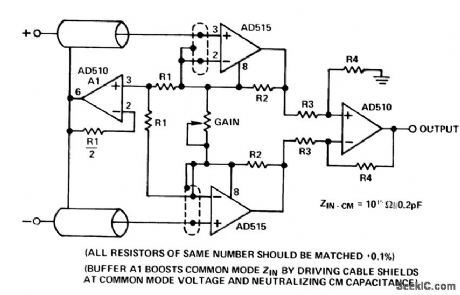
Very-high impedance instrumentation amplifier using two AD510s and two AD515s (courtesy Analog Devices, Inc.). (View)
View full Circuit Diagram | Comments | Reading(731)
Commutator_network_using_N_channel_MOSFETs
Published:2009/7/21 3:11:00 Author:Jessie
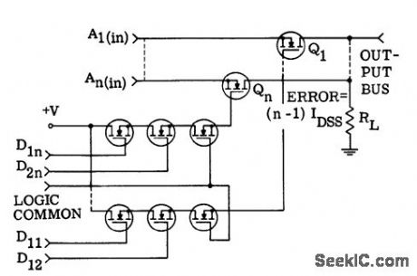
Commutator network using N-channel MOSFETs. All semiconductors are 2N4351s. Each switch has a three-input AND gate in series with the gate drive (courtesy Motorola Semiconductor Products Inc.). (View)
View full Circuit Diagram | Comments | Reading(842)
Precision_high_CMV
Published:2009/7/21 3:09:00 Author:Jessie
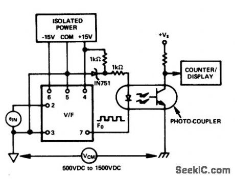
Precision high CMV (common mode voltage) analog isolator. This circuit provides up to 1500 volts DC CMV isolation (courtesy Analog Devices, Inc.). (View)
View full Circuit Diagram | Comments | Reading(688)
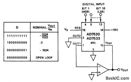
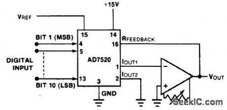
Four_quadrant_multiplication_with_the__in_bipolar_operation
Published:2009/7/21 3:09:00 Author:Jessie
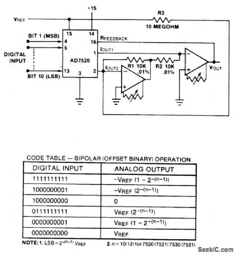
Four-quadrant multiplication with the AD7520 in bipolar operation. The Intersil AD7520 is an 18-pin multiplying D/A converter. A logic one input at any digital input forces the corresponding ladder switch to steer the bit current to the IOUT1 bus. A logic zero input forces the bit current to the IOUT2 bus. For any code the IOUT1 and IOUT2 bus currents are complements of one another. The current amplifier at IOUT2 changes the polarity of IOUT2 current and the transconductance amplifier at lour output sums the two currents. This configuration doubles the output range but halves the resolution of the D/A convener. For the offset adjustment set VREF to approximately +10 volts and connect all digital inputs to logic one. Adjust the IOUT2 amplifier offset zero pot for 0V ±1 mV at IOUT2 amplifier output. Connect the MSB to logic one and all other bits to logic zero. Adjust IOUT1 offset zero pot for 0V ±mV at VOUT. For the gain adjustment connect all digital inputs, to VDD. Monitor VOUT for a -VREF (1- 2- (n - 1)) volt reading, where n is equal to 10. To increase VOUT connect a series resistor, 0 to 500 ohms, in the lour amplifier feedback loop. To decrease VOUT connect a series resistor, 0 to 500 ohms, between the reference voltage and pin 15 (courtesy Intersil, Inc.). (View)
View full Circuit Diagram | Comments | Reading(1152)
45_MHz_color_TV_sound_IF_amplifier_using_ECG703A
Published:2009/7/21 3:49:00 Author:Jessie
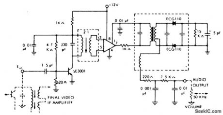
4.5 MHz color TV sound IF amplifier using ECG703A. In a color TV the 4.5 MHz IF is not generated in the video detector as in B&W sets. A separate transistor sound detector, driven from thefinal video IF amplifier, is used to develop the 4.5 MHz IF. The drivertransformer at the input of the chip is tuned to 4.5 MHz. The output drives a conventional ratio detector, which provides good AM rejection well belowfull limiting (courtesy GTE Sylvania Incorporated).
(View)
View full Circuit Diagram | Comments | Reading(1558)
Variable_gain_amplifier
Published:2009/7/21 3:48:00 Author:Jessie
Variable gain amplifier (two-quadrant divider). Examples of gains at various codes are given in the table (courtesy Analog Devices, Inc.). (View)
View full Circuit Diagram | Comments | Reading(0)
Complete_RGB_video_output_stage_for_color_TV_using_the_ECG713_chip
Published:2009/7/21 3:45:00 Author:Jessie
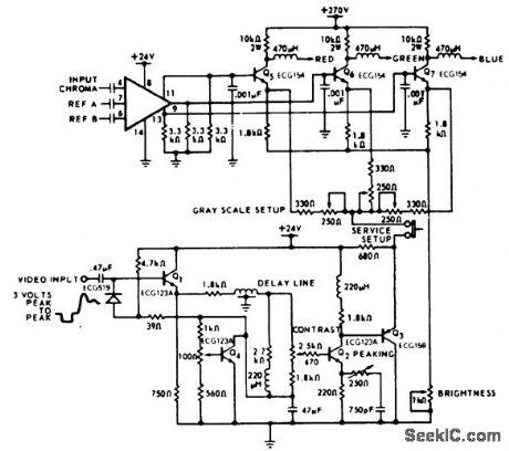
Complete RGB video output stage for color TV using the ECG713 chip (courtesy GTE Sylvania Incorporated). (View)
View full Circuit Diagram | Comments | Reading(663)
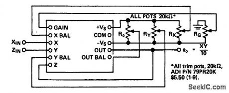
Vector_computation_circuit_for_n_variables_using_three_434_multiplier_dividers_and_two_AD741_op_amps
Published:2009/7/21 3:43:00 Author:Jessie
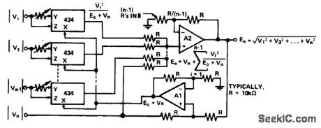
Vector computation circuit for n variables using three 434 multiplier/dividers and two AD741 op amps (courtesy Analog Devices, Inc.). (View)
View full Circuit Diagram | Comments | Reading(862)
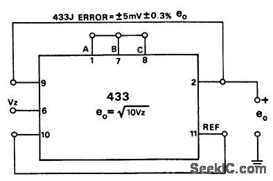
Vector_computation_circuit_for_VC2_=_VA2___VB2_using_the_433_multiplier_divider_and_two_AD741_op_amps
Published:2009/7/21 3:42:00 Author:Jessie

Vector computation circuit for VC2 = VA2 + VB2 using the 433 multiplier/divider and two AD741 op amps (courtesy Analog Devices, Inc.). (View)
View full Circuit Diagram | Comments | Reading(681)
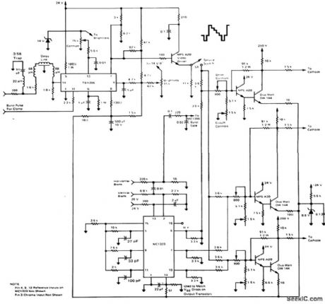
358_MHz_injection_locked_oscillator_for_color_TVUsing_one_ECG703A_IC
Published:2009/7/21 3:41:00 Author:Jessie
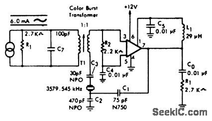
3.58 MHz injection-locked oscillator for color TV,Using one ECG703A IC. The burst transformer induces the chroma reference directly intothefeedback loop of the oscillator, thereby locking the oscillator in phase with the transmitted burst (courtesy GTE Sylvania Incorporated). (View)
View full Circuit Diagram | Comments | Reading(1088)
Square_root_of_the_sum_of_the_squares_circuit
Published:2009/7/21 3:40:00 Author:Jessie

Square root of the sum of the squares circuit. This circuit performs vector computations (courtesy Analog Devices, Inc.). (View)
View full Circuit Diagram | Comments | Reading(1172)
Multiplier_circuit_using_the_435_multiplier_divider_chip
Published:2009/7/21 3:37:00 Author:Jessie
Multiplier circuit using the 435 multiplier/divider chip (courtesy Analog Devices, Inc.). (View)
View full Circuit Diagram | Comments | Reading(704)
Square_rooter_using_the_433_multiplier_divider_chip
Published:2009/7/21 3:37:00 Author:Jessie
Square rooter using the 433 multiplier/divider chip (courtesy Analog Devices, Inc.). (View)
View full Circuit Diagram | Comments | Reading(725)
Square_rooter_circuit_using_the_434_multiplier_divider_chip
Published:2009/7/21 3:36:00 Author:Jessie
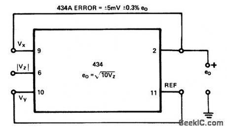
Square rooter circuit using the 434 multiplier/divider chip (courtesy Analog Devices, Inc.). (View)
View full Circuit Diagram | Comments | Reading(696)
Pulse_width_modulator_using_an_ECG955M_timer_oscillator_chip
Published:2009/7/21 3:35:00 Author:Jessie
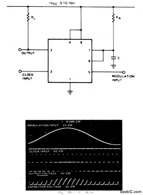
Pulse width modulator using an ECG955M timer/oscillator chip. The flip-flop is connected in a monostable mode. The circuit is triggered with a continuous pulse train and the threshold voltage is modulated by the signal applied to control voltage pin 5. This has the effect of modulating the pulse width as control voltage varies (courtesy GTE Sylvania Incorporated). (View)
View full Circuit Diagram | Comments | Reading(890)
Two_quadrant_multiplication_with_the_AD7520_in_unipolar_binary_operation
Published:2009/7/21 3:34:00 Author:Jessie
Two-quadrant multiplication with the AD7520 in unipolar binary operation. The Intersil AD7520 is an 18-pin multiplying D/A converter. To adjust the zero offset connect all digital input to ground, and adjust the zero trimmer on the op amp for 0V ± 1 mV at VOUT. To adjust the gain connect all digital inputs of the AD7520 to VDD. Monitor VOUT for a -VREF ( 1 - 2-n ) reading, where n is equal to 10. To decrease VOUT connect a series resistor, 0 to 500 ohms, between the reference voltage and pin 15. To increase VOUT connect a series resistor, 0 to 500 ohms, in the VOUT1 amplifier feedback loop (courtesy Intersil, Inc.). (View)
View full Circuit Diagram | Comments | Reading(789)
Color_TV_complete_video_amplifier_system_featuring_DC_contrast_and_brightness_DC_restorer_for_black_level_clamping_ganged_contrast_and_color_controls_and_ABL
Published:2009/7/21 7:05:00 Author:Jessie
Color TV complete video amplifier system featuring DC contrast and brightness, DC restorer for black-level clamping, ganged contrast and color controls and ABL (courtesy Motorola Semiconductor Products Inc.). (View)
View full Circuit Diagram | Comments | Reading(1203)
TV_horizontal_processor_with_phase_detector_oscillator_and_predriver
Published:2009/7/21 6:23:00 Author:Jessie
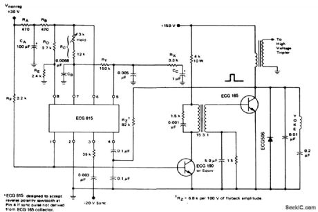
TV horizontal processor with phase detector, oscillator, and predriver. Suited for all types of TV receivers, this circuit features internal shunt regulator, preset hold control capability, ±300-hertz pull-in, linear balanced phase detector, variable output duty cycle for driving tube or transistor, low thermal frequency drift, adjustable DO loop gain and positive flyback inputs (courtesy GTE Sylvania Incorporated). (View)
View full Circuit Diagram | Comments | Reading(2277)
Complete_TV_sound_system_that_provides_approximately_2_watts_ofaudio_power
Published:2009/7/21 4:51:00 Author:Jessie
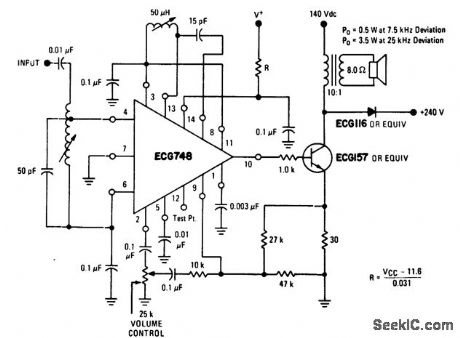
Complete TV sound system that provides approximately 2 watts ofaudio power.Sound detection is accomplished through a coincidence discriminatorin thechipthat requlres only one RLC phase shift network,supply for the chip should be approximately 16 volts,Selectthe value of resistor R toobtain 11.6 volts at pin 14 ofthe ECG748(courtesy GTE Sylvania Incorporated). (View)
View full Circuit Diagram | Comments | Reading(718)
| Pages:35/126 At 202122232425262728293031323334353637383940Under 20 |
Circuit Categories
power supply circuit
Amplifier Circuit
Basic Circuit
LED and Light Circuit
Sensor Circuit
Signal Processing
Electrical Equipment Circuit
Control Circuit
Remote Control Circuit
A/D-D/A Converter Circuit
Audio Circuit
Measuring and Test Circuit
Communication Circuit
Computer-Related Circuit
555 Circuit
Automotive Circuit
Repairing Circuit