
Measuring and Test Circuit
Index 61
MICROPOWER_RADIOACTIVE_RADIATION_DETECTOR
Published:2009/7/5 23:51:00 Author:May
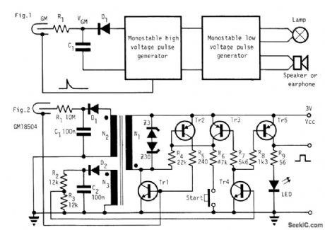
Circuit NotesIn the absence of radiation, no current is drawn. At normal background radiation levels the power consumption is extremely low. The instrument may be left on for several months without changing batteries. In this way the detector is always ready to indicate an increase in radiation. An LED is used as an indicator lamp. With background radiation it draws less than 50 μA ferrite pot core is used for the transformer with N1=30, N2=550, and N3=7. Using two 1.5V batteries with 0.5 Ah total capacity, the detector can work at background radiation levels for 0.5 Ah + 50μA=10,000 hours, which is more than a year. (View)
View full Circuit Diagram | Comments | Reading(1135)
55_MHz_presettable_counter
Published:2009/7/5 23:34:00 Author:May
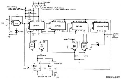
High-speed four-decade counter with preload switches gives positive output pulse 30 ns long at 55 MHz to ensure that all counters are preset to right digit and transients have died out at end of count. If counters are preset to 5555, input fre-quency is counted until countgets to 9997. Next clock pulse triggers auxiliary flip-flop to initiate load pulse (2 cycles long) and get back tozero Total count is 10,000 minus 5555, or 4445 (10-kHz output for 44.5-MHz input.) Article covers construction and testing. Counter draws less than 300 mA at 5 V. Developed for use in 2-meter frequency synthesizer-H. Cross, HighSpeed Divide-by-N Counters, Ham Radio, March 1976, p 36-38. (View)
View full Circuit Diagram | Comments | Reading(1475)
SINPLE_PHASE_DETECTOR_CIRCUIT
Published:2009/7/5 23:16:00 Author:May
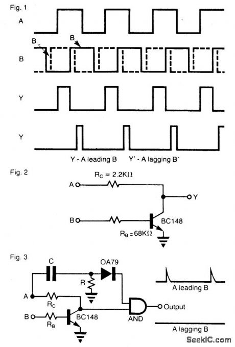
The operation of the circuit is like an enabled inverter, that is, the output Y=B provided A is high. If A is low, output is low (independent of the state of B). When the signals A and B or B1 are connected to the inputs A and B of this gate the output Y is a pulse train signal (shown a Y or Y1) which has a pulse duration equal to the phase difference between the two signals. The circuit is directly suitable for phase difference measurement from zero to 180°. This performance is similar to the circuits like the Exclusive OR gate used for this purpose. With this method leading and lagging positions of the signals can also be found using an AND gate. Phase difference measured along with the leading and lagging information gives complete information about the phases of the two signals between zero and 360°. (View)
View full Circuit Diagram | Comments | Reading(1242)
PHASE_SEQUENCE_DETECTOR_II
Published:2009/7/5 23:15:00 Author:May
This circuit derives its supply voltage, VCC and Vdd from φC. This factor, together with the neon lamps and zener diodes in the phase inputs, establishes 50% threshold that detects low voltage or absence of one or more phases. Relay K1 energizes for correct phase volts. (View)
View full Circuit Diagram | Comments | Reading(1676)
FLASHING_LED_IS_REMOTE_MONITOR
Published:2009/7/5 23:14:00 Author:May
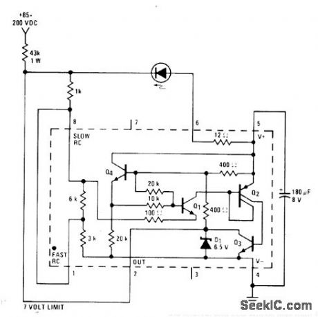
Circuit uses National LM3909 flasher IC to drive LED for monitoring remotely located high-voltage power supply. When 43K dropping resistor is located at power supply, all other voltages on the line, IC, and LED will be less than 7 V above ground, for safe remote monhoring. Use any LED drawing less than 150 mA.-P. Lefferts, Power-Miser Flasher IC Has Many Novel Applications, EDN Magazine, March 20, 1976, p 59-66. (View)
View full Circuit Diagram | Comments | Reading(830)
THREE_PHASE_TESTER
Published:2009/7/5 23:13:00 Author:May
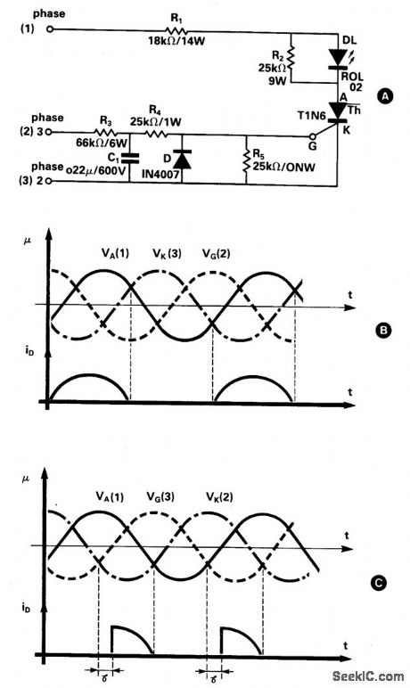
This simple three-phase tester, uses only a small current thyristor as a main element for testing the right or wrong succession of the three phases, and there is no need for a supplementary power supply.
The basic circuit is shown in Fig. 69-4A. When connecting to the thyristor anode, grid, and cathode the three phases of the supply network in the sequence phase L, phase 3, phase 2, are considered as correct, the mean value of the current through the thyristor is relatively high (since it is turned on during an entire half-period of one phase). The result is that the LED will emit a normal light.
The wave shapes for the three voltages and the current through the LED for this situation are shown in Fig. 69-4B.
If the three phases are not correctly connected-phase 1 to the anode, phase 2 to the grid, and phase 3 to the cathode, for instance-the thyristor will be turned on for a very short time and the LED will produce a very poor light. The wave shapes for this case are shown in Fig. 69-4C. The delay time is given by the R3-R1-R4 group.
When any of the three phases is missing, there is no current through the thyristor and the LED will emit no light. (View)
View full Circuit Diagram | Comments | Reading(2647)
PHASE_SEQUENCE_DETECTOR
Published:2009/7/5 23:11:00 Author:May
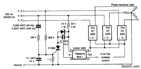
This circuit prevents damage to the load due to incorrect phasing. The three power SSR's are only permitted to turn-on for a phase sequence of phase A leading phase B.
If phase A lags phase B the input currents will cancel, causing the SCR and the inhibit SSR to remain off until the sequence is reversed. The inhibit SSR is included to maintain isolation at the input. (View)
View full Circuit Diagram | Comments | Reading(4957)
PEAK_DETECTOR
Published:2009/7/5 23:07:00 Author:May
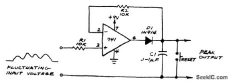
The comparator will charge C1 until the voltage across the capacitor equals the mputvoltage. If subsequent utput vo⒒age exceeds that stored In C1,the comparator voltagewill go high and charge C1 to new higher peak voltage (View)
View full Circuit Diagram | Comments | Reading(0)
POSITIVE_PEAK_DETECTOR
Published:2009/7/5 23:07:00 Author:May
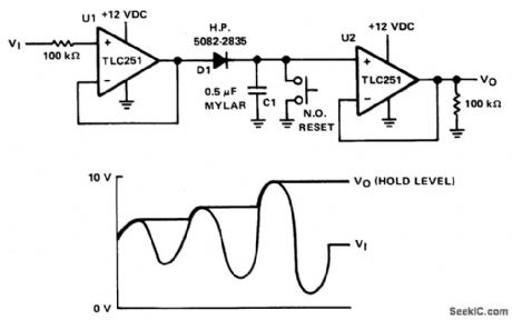
The purpose of the circuit is to hold the peak of the input voltage on capacitor C1, and read the value, VO, at the output of U2. Op amps UI and U2 are connected as voltage followers. When a signal is applied to VI, C1 will charge to this same voltage through diode D1. This positive peak voltage on C1 will maintain VO at this level until the ca-pacitor is reset (shorted). Of course, higher positive peaks will raise this level while lower power peaks will be ignored. C1 can be reset manually with a switch, or electronically with an FET that is normally off. The capacitor specified for C1 should have low leakage and low dielectric absorption. Diode D1 should also have low leakage.
Peak values of negative polarity signals may be detected by reversing D1. (View)
View full Circuit Diagram | Comments | Reading(0)
CAPACITOR_TESTER
Published:2009/7/5 22:48:00 Author:May
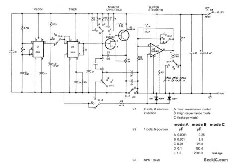
Portable instrument measures capacitance values to 2500μF and leakage current with up to 8 V applied. Timer U1 operates as clock providing about 350 negative-going pulses per second to trigger timer U2 and unclamp test capacitor so it charges through switch-selected resistor to half of supply voltage. U2 then resets, discharging capacitor through pin 7. During charge, pin 3 of U2 is high (about 8 V) and duration of high state is directly proportional to capacitance. Resulting rectangular waveform is applied to unity-gain buffer opamp U3 that feeds meter through calibrating trimpot R6. Meter deflection is proportional to average value of rectangular output waveform and is therefore proportional to capacitance. Table gives switch functions. Mode B uses larger clock timing capacitor to permit measuring larger capacitance values, for total of10 ranges Article covers construction,calibration and use.-P. H. Mathleson, Wide-Range Capacitance Meter, Ham Radio, Feb.1978,p51-53 (View)
View full Circuit Diagram | Comments | Reading(3232)
1_pF_TO_1_μF
Published:2009/7/5 22:46:00 Author:May
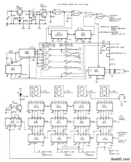
Presents instantly in digital form the value of unknown capacitor, in ranges of 1-9999 pF and 1-999.9 nF. Four digits are displayed, with leading-zero suppression and overflow indicator. Accuracy is better than 0.1% of full range ±1 digit for higher values in both ranges. Mono MVBR IC21 produces pulse whose length is directly proportional to value of CX plus about 980-pF total in CF. This pulse enables gate IC14D whose output goes to counter. Oscillator Q2, buffer Q3, dividers IC15 and IC16, and gates IC14 together give 40-MHz (range 1) or 400-kHz (range 2) pulses that are counted while IC21 holds IC14D open. Article covers construction in detail.-I. M. Chladek, Build This Digital Capacity Meter, 73Magazine, Jan. 1976, p 70-78. (View)
View full Circuit Diagram | Comments | Reading(1385)
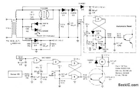
GAS_SMOKE_DETECTOR_WITH_BEEPING_HORN
Published:2009/7/5 22:42:00 Author:May
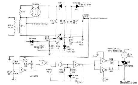
Taguchi TGS308 gas sensor increases voltage across R3 when sensor conductivity is increased by combustible gases. After time delay provided to prevent power tumon false alarms, CMOS astable MVBR using gates 3 and 4 is energized to fire triac and drive AC horn to give distinctive repetitive sound lasting about 2.5 s, with 0.2-s intervals between beeps. Triac gate drivers operate from -15 V supplyderived from 24-V winding of power transformer.-A.Pshaenich, Solid State Gas/Smoke Detector Systems, Motorola, Phoenix, AZ, 1975, AN-735, p 6. (View)
View full Circuit Diagram | Comments | Reading(2463)
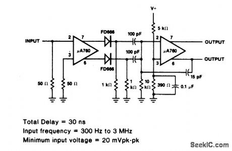
RECEIVER_FOR_50_kHz_FM_OPTICAL_TRANSMITTER
Published:2009/7/5 22:41:00 Author:May
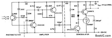
For maximum range, the receiver must be designed in the same manner as a radio receiver front end, since the received signals will be similar in both frequency component and in amplitude of the photodiode current. The major constraint on the receiver performance is signal to noise ratio, followed by e.m. shielding, stability, bias points, parts layout, etc. These become significant details in the final design. This receiver circuit consists of a L14G2 detector, two stages of gain, and a FM demodulator which is the tachometer circuit, modified to operate up to 100 kHz. Better sensitivity can be obtained using more stages of stabilized gain with AGC, lower cost and sensitiity may be obtained by using an H23A1 emitter-detector pair and/or by eliminating amplifter stages.
For some applications, additional filtering of the output voltage may be desired. (View)
View full Circuit Diagram | Comments | Reading(2303)
ZERO_CROSSING_DETECTOR_2
Published:2009/7/5 22:40:00 Author:May
View full Circuit Diagram | Comments | Reading(701)
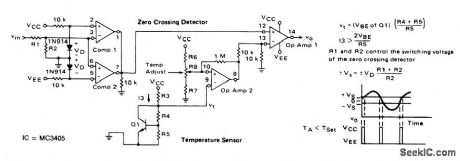
ZERO_CROSSING_DETECTOR_WITH_TEMPERATURE_SENSOR
Published:2009/7/5 22:39:00 Author:May
View full Circuit Diagram | Comments | Reading(1039)
ZERO_CROSSING_DETECTOR
Published:2009/7/5 22:38:00 Author:May
View full Circuit Diagram | Comments | Reading(0)
ZERO_CROSSING_DETECTOR_1
Published:2009/7/5 22:38:00 Author:May
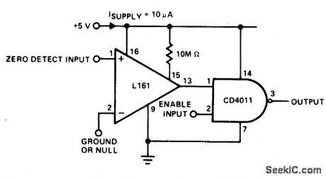
This detector is useful in sine wave squaring circuits and A/D converters. The positive input may either ve grounded or connected to a nulling voltage which cancels input offsets and enables accuracy to within microvolts of ground. The CMOS output will switch to within a few millivolts of either rail for an input voltage change of less than 200 μV. (View)
View full Circuit Diagram | Comments | Reading(882)
GAS_SMOKE_DETECTOR_WITH_LATCH
Published:2009/7/5 22:36:00 Author:May
CMOS latching logic provides 2-min time delay to prevent false alarm when power is first applied to fire alarm using Taguchi TGS308 gas sensor whose conductivity increases in presence of combustible gases. Normal voltage of 3 VRMS across R4 increases to about 20 V in presence of fire. Half of 12.6-V center-tapped transformer secondary is used for 6-V supply and full 12.6 V for DC horn supply. Latch is reset manually with S1 to turn off alarm after gas level drops. Optional circuit shown can be used for automatic reset.-A, Pshaenich, Solid State Gas/Smoke Detector Systems, Motorola, Phoenix, AZ, 1975, AN-735, p 5. (View)
View full Circuit Diagram | Comments | Reading(1762)
ZERO_CROSSING_DETECTOR
Published:2009/7/5 22:34:00 Author:May
View full Circuit Diagram | Comments | Reading(0)
SMOKE_DETECTOR
Published:2009/7/5 22:31:00 Author:May
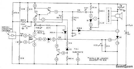
Battery-operated ionization-type srnoke detector uses RCA CA3130 opamp as interface for ionization chamber that provides picoampere currents. With opamp in pulsed mode (on for 20 ms of 20-s period), IC draws only 0.6 μA average instead of 600 μA.Other active components and zener, all on RCA CA3097 array, provide Low-battery monltor and horn-driver functions. When chamber detects smoke, combination of RF and D1 provides sufficient base current to keep Q3 and Q4 on.Opamp is then powered continuously, and steering diode Z1 supplies continuous current to gate of Q2 for energizing hom. Battery drain is only 5 mA in monitoring mode.-G. J. Granieri, Bipolar-MOS and Bipolar IC's Buildlng Blocks for Smoke-Detector Circuits, IEEE Transactions on Consumer Electronics, Nov. 1977, p 522-527.
(View)
View full Circuit Diagram | Comments | Reading(2552)
| Pages:61/101 At 206162636465666768697071727374757677787980Under 20 |
Circuit Categories
power supply circuit
Amplifier Circuit
Basic Circuit
LED and Light Circuit
Sensor Circuit
Signal Processing
Electrical Equipment Circuit
Control Circuit
Remote Control Circuit
A/D-D/A Converter Circuit
Audio Circuit
Measuring and Test Circuit
Communication Circuit
Computer-Related Circuit
555 Circuit
Automotive Circuit
Repairing Circuit