
power supply circuit
Index 38
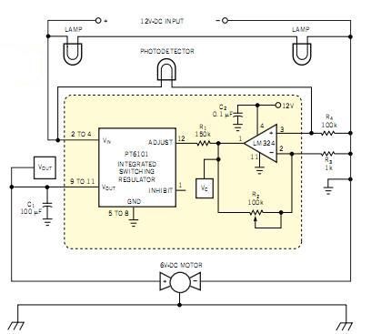
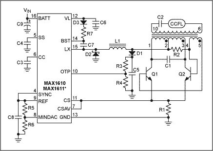
Switching regulator drives robot motor
Published:2012/11/9 20:24:00 Author:muriel | Keyword: Switching regulator, robot motor
View full Circuit Diagram | Comments | Reading(886)
A very STABLE 40khz generator
Published:2012/11/9 0:31:00 Author:muriel | Keyword: A very STABLE, 40khz, generator
A circuit that I have used before is based on the CD4060 (14stage binary counter) and a 640Khz ceramic resonator. The CD4060 is basically an oscillator and a ripple counter to divide the 640khz down to something more usable.
Here is the pinout of the CD4060 (frequencies are assuming a 640khz input signal into pins 10/11/12 - circuit shown below):
+-\/-+
160hz 1 | | 16 Vcc
80hz 2 | | 15 625hz
40hz 3 | | 14 2.5khz
10khz 4 | | 13 125hz
20khz 5 | | 12 \
5khz 6 | | 11 >---- see sub-circuit below
40khz 7 | | 10 /
GND 8 | | 9 NC
+----+
Sub-circuit for a 640khz ceramic resonator:
12 >----------------------+
740pf | (you may be able to obtain
11 >-------+----+---|(----+ a resonator with builtin
| | | capacitors and three leads)
640khz --- \ |
res. O / 1Mohm |
--- \ |
| | |
10 >-------+----+---|(----+
740pf |
GND >----------------------+
A nice part about this circuit is that it delivers a STABLE 40khz signal, as well as delivering several other frequencies that can be used to modulate the 40khz carrier. For example, the person that designed this circuit (Ken Boone, member of Triangle Amateur Robotics) used it to build several beacons in his yard to serve as navigation points for a robotic lawnmower. By diode-OR'ing the results of the 40khz carrier and one of the lower frequencies (such as the 125Hz) line to drive a ring of IR-LEDs, he could locate the beacon and tell which, of several, beacons he had found.
This circuit has proven to be VERY stable, and is fairly inexpensive (about $1.50 for the CD4060 and 640Khz ceramic resonator). (View)
View full Circuit Diagram | Comments | Reading(1010)
Tripler Converts 5V to 15V
Published:2012/11/9 0:11:00 Author:muriel | Keyword: Tripler , 5V to 15V
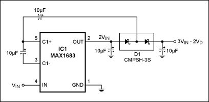
This application note shows how to configure the MAX1683 to triple the input voltage for low-current applications while minimizing voltage drop.
A similar version of this article appeared in the August 17, 2000 issue of ECN magazine.
By configuring a charge-pump voltage doubler as a tripler, you can readily derive 15V from 5V. A 15V rail is useful for powering op amps, LCD-bias circuits, and other low-current applications.
The connections in Figure 1 configure the MAX1683 voltage doubler as a tripler. The no-load output voltage of the circuit is approximately 3VIN - 2VD, where VD is the voltage drop across one diode. Use Schottky diodes as shown to minimize VD and its effect on output voltage. (View)
View full Circuit Diagram | Comments | Reading(1181)
Triple Capacitive Voltage Inverter with the MAX871
Published:2012/11/9 0:10:00 Author:muriel | Keyword: Triple Capacitive Voltage , Inverter, MAX871
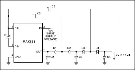
This design idea is based on a customer request for a cheap, and not very accurate, negative voltage supply of about -12V to -15V with a low output current of < 5mA and an input voltage of 5V. This application might be used for negative op-amp supply. Figure 1 shows the typical operation circuit with the flying capacitor C1 and C2. The output voltage on pin 1 is -VIN. Four additional capacitors (C3 to C6) and four additional diodes (D1 to D4) triple the negative output voltage at the OUT pin from -VIN to -3VIN. C5 and C6 decreases the voltage with every step by -VIN. Without any diode voltage drop C3 got -2VIN and C4 charges ideally to -3VIN. It is possible to add more of these cascades but with every step the voltage drop of the diodes will reduce the effort. (View)
View full Circuit Diagram | Comments | Reading(1067)
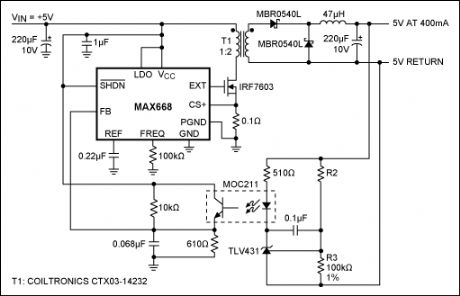
DC-DC Boost Converter plus LDO
Published:2012/11/9 0:09:00 Author:muriel | Keyword: DC-DC , Boost Converter , LDO
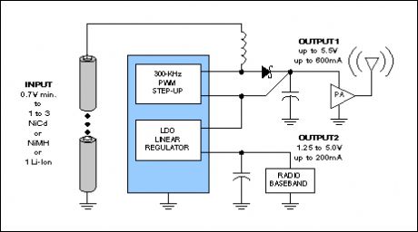
Combining a DC-DC boost converter with an LDO has two advantages: It implements a low-noise boost function (at a slight penalty in efficiency versus the noisy booster without an LDO), and it performs the buck/boost function with surprisingly high efficiency. A typical buck/boost application converts the output of one Li-ion cell to 3.3V. Efficiency is very high, because the battery spends most of its life near 3.6V, allowing the booster to idle and providing the LDO with a near-ideal input voltage. This system also delivers higher efficiency with smaller external components than the traditional SEPIC converter. Because of the favorable characteristics of this arrangement, several single-chip implementations are available for the DC-DC boost converter plus LDO architecture. (View)
View full Circuit Diagram | Comments | Reading(1752)
Regulated Charge Pump Delivers 50mA
Published:2012/11/9 0:07:00 Author:muriel | Keyword: Charge Pump, 50mA
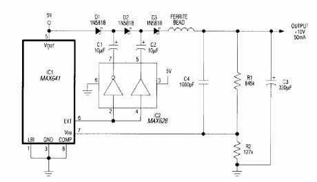
The DC-DC converter circuit of Figure 1 substitutes a voltage tripler in place of the external inductor and diode normally associated with switching regulator IC1. Inverting and noninverting drivers in the MOSFET-driver chip (IC2) activate a diode/capacitor tripling network (D1-D3, C1-C3). In comparison with charge pumps based on single-polarity drivers, the buffer/inverter combination of IC2 enables this circuit to deliver more current with fewer parts.A 50kHz oscillator within IC1 produces the EXT signal (pin 6), which IC2 converts to drive signals (180° out of phase) for the tripler. The resulting charge-discharge action in the capacitors recharges C3 toward 10V every 20µs. The ferrite bead limits output ripple to about 20mVP-P for a 50mA load. (View)
View full Circuit Diagram | Comments | Reading(1305)
One 9V battery gives +18, +25, +33V
Published:2012/11/9 0:06:00 Author:muriel | Keyword: One , 9V, battery , +18, +25, +33V
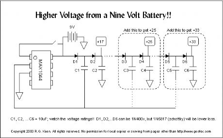
For you high-voltage minibooster fans out there, here's the one-chip, one battery way to do it.
The MAX1044 is a charge pump converter - it uses a capacitor as a bucket to pump charge from one place to another. Normally, there is a capacitor connected from pin 2 of the 1044 to pin 4. This capacitor is charged between +9V and ground, and then switched in parallel with a capacitor from pin 5 to ground in a way that makes a negative voltage on the second cap.
In this UPverting use, the 1044 still switches pin 2 between +9V and ground just as it would for a voltage inverter. However, we ignore the pin 4 and 5 connections that would make an inverter from it. Instead, we connect two capacitors and diodes as shown (D1, 2, and C1, 2). The voltage on pin 2 of the 1044 is switched from +9V to ground. When it switches to ground, C1 fills with voltage through D1. When it then switches to +9, it pulls the negative terminal of C1 up to +9V. D1 now blocks any flow of current back into the battery, so the charge in C1 flows through D2 into C2. So at C2, we now get almost 18V!
There's more. If we add another two diodes and capacitors (D3, D4 and C3, C4), we can add another 9V to it, as C3 charges to +18 through D3 when pin 2 is at ground, and is pulled up to +25 (+27 minus the voltage drops of the diodes) when pin 2 goes high. We can do it again with D5, D6 and C5, C6 to get +33V. The limit on all this is the losses in the diode voltages. Each time we add a section, we add two more diode drops that we can't take advantage of to charge capacitors. But +33 is not bad for a single 9V battery!
If you build this, you MUST take notice of the voltages on the capacitors. The caps can all be the same value, but C1, C2 need to be 25V units, C3, 4, 5, and 6 can be 35V units, and C5 and C6 might need to be 50V unit just for some safety margin. 1N400x diodes work and are cheap, but the losses are higher than they really need to be. For higher performance and lower losses, it's better to use something like the 1N5817 schottky diodes for low losses. But both will work.
This charge pumping is a very efficient way to convert voltages. The only power lost is that power dissipated in the resistances of the switches inside the 1044 and the series resistance of the capacitors and diodes, as well as the power to run the internal oscillator that flips the switches when needed.
All by itself, the 1044 runs at about 7-10kHz, so there will be ripple of that amount on the C2 output and on the +9V output from the battery as well. Audio equipment that uses this voltage could have a whine audible if you're not careful. However, the 1044 has a frequency boost feature. If you connect pin 1 to the power supply (shown by the little open switch) then the oscillator frequency goes up by about 6:1. The oscillator then works well above the audio region. Any whine is then going to be inaudible. (View)
View full Circuit Diagram | Comments | Reading(1222)
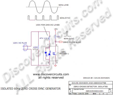
Fully Isolated 50/60Hz Sync Generators
Published:2012/11/8 1:33:00 Author:muriel | Keyword: Fully, Isolated, 50/60Hz , Sync Generators
View full Circuit Diagram | Comments | Reading(891)
Choosing the Right Power-Supply IC for your Application
Published:2012/11/8 1:27:00 Author:muriel | Keyword: Power-Supply IC
Choosing a power-supply IC can be a daunting task for the inexperienced. This application note will help the novice engineer take the first step toward becoming a confident power-supply designer. This article discusses how to choose these ICs at the most fundamental level. First, it explains why power-supply ICs are necessary. It then shows how to choose among the three most common power-supply ICs powered with DC voltages: linear regulators, switching regulators, and charge pumps. Links to supportive application notes and tutorials will address more advanced power-supply topics. (View)
View full Circuit Diagram | Comments | Reading(993)
Charge Pump Doubles Negative Voltage
Published:2012/11/8 1:26:00 Author:muriel | Keyword: Charge Pump , Doubles Negative, Voltage
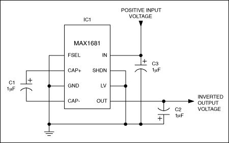
For low-power dc-dc circuits, the small size and high efficiency of charge pumps makes them ideal for simple doubling and inverting applications. The absence of such ICs designed for negative voltage, however, requires that you adapt an existing positive-voltage device.
(View)
View full Circuit Diagram | Comments | Reading(1921)
Charge-Pump and Step-Up DC-DC Converter Solutions for Powering White LEDs in Series or Parallel Connections
Published:2012/11/8 1:25:00 Author:muriel | Keyword: Charge-Pump , Step-Up, DC-DC Converter Solutions
View full Circuit Diagram | Comments | Reading(1374)
Boost Converter Generates Three Analog Rails
Published:2012/11/8 1:21:00 Author:muriel | Keyword: Boost Converter, Three Analog Rails
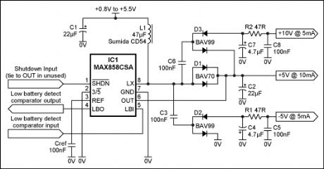
In Figure 1, a standard boost converter consisting of IC1, C1, L1, D1, and C2 generates, in addition to the main output, two auxiliary supply rails (10V and -5V) with the addition of some small and very low-cost extra components. Such rails are useful for the analog circuitry in small handheld instruments, which often require supply voltages in excess of the signal range.The main regulated output of 5V ±2% is sustained by input voltages in the range 0.8V to 5.5V (i.e., from a battery pack of 1 to 3 cells). With an input of 1.8V (two flat cells) and the other rails unloaded, it can produce 25mA with a high efficiency of 80% to 90%.The -5V and 10V outputs are derived from low-cost, discrete charge pumps driven by the converter's switching node (LX) via flying capacitors C3 and C6. The LX node switches between 0V and a level one diode drop above the 5V rail, so the charge pumps' drive voltage is reasonably well regulated. Moreover, the drop across D1 somewhat compensates for diode drops in the two charge-pump outputs.Even more useful is the behavior of IC1 with an increasing load on the auxiliary rails. Its internal control scheme (current-limited, minimum-off-time, pulse-frequency modulation) constantly adapts its switching frequency to the net load current drawn from the rails: frequency increases when the load increases, producing a greater transfer of energy via the flying capacitors. The result is a sort of pseudo-regulation for the charge-pump outputs.These analog supply rails are intended for driving precision op amps, whose input CMR and output range are 2V to 3V within the supply rails. Thus, the rails are good enough if the -5V output is below -3V and the 10V output is above 8V. Accordingly, the components shown were chosen for minimum cost and lowest ripple rather than maximum regulation. Examples are the lossy RC output filters, and the choice of silicon signal diodes instead of Schottky diodes. The 4.7µF capacitors C4 and C7 can be high-ESR, commodity multilayer ceramic types with 16V rating, 1206 case, and Y5V dielectric—such as the 1206YG475ZAT2A from AVX.Output ripple varies with the supply voltage and output load. Operating with an input voltage of 1.8V, the circuit produces ripple amplitudes over the load range of 2mV to 10mVp-p for the 10V rail and 15mV to 30mVp-p for the -5V rail. By increasing C5 and C8 to 2.2µF, you can reduce these ripple levels to 1mV and 5mV respectively. (View)
View full Circuit Diagram | Comments | Reading(848)
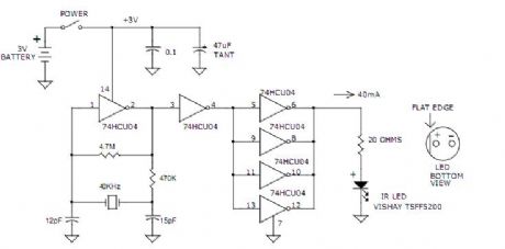
40KHZ LED TEST SIGNAL GENERATOR
Published:2012/11/8 1:19:00 Author:muriel | Keyword: 40KHZ, LED , TEST SIGNAL, GENERATOR
View full Circuit Diagram | Comments | Reading(1096)
100mA Ultralow Noise Charge Pump LED Supply
Published:2012/11/8 1:18:00 Author:muriel | Keyword: 100mA , Ultralow Noise , Charge Pump, LED Supply
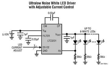
View full Circuit Diagram | Comments | Reading(961)
CMOS INVERTERS FORM 125KHZ OSCILLATORS
Published:2012/11/8 1:17:00 Author:muriel | Keyword: CMOS, INVERTERS, 125KHZ OSCILLATORS
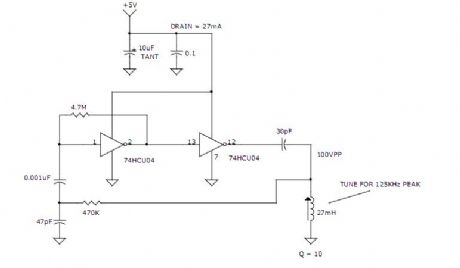
View full Circuit Diagram | Comments | Reading(1288)
CHARGE PUMP EFFICIENTLY DIVIDES SUPPLY VOLTAGE
Published:2012/11/8 1:16:00 Author:muriel | Keyword: CHARGE , PUMP EFFICIENTLY , DIVIDES SUPPLY VOLTAGE
View full Circuit Diagram | Comments | Reading(1056)
AUDIO FREQUENCY DIGITAL NOISE GENERATORS
Published:2012/11/8 1:14:00 Author:muriel | Keyword: AUDIO FREQUENCY , DIGITAL NOISE , GENERATORS
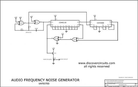
When you need to test an audio circuit with broadband noise, this circuit works great. It uses just three inexpensive C-MOS ICs that generate a series of output pulses whose widths vary randomly. I included a level control pot. (View)
View full Circuit Diagram | Comments | Reading(990)
200MHz to 400MHz VOLTAGE CONTROLLED OSCILLATOR
Published:2012/11/8 1:12:00 Author:muriel | Keyword: 200MHz to 400MHz , VOLTAGE CONTROLLED OSCILLATOR
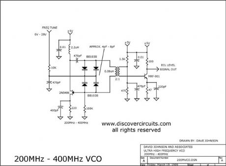
View full Circuit Diagram | Comments | Reading(2141)
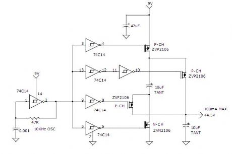
+5v Powered Charge Pump Battery Charger
Published:2012/11/8 1:10:00 Author:muriel | Keyword: +5v , Powered Charge , Pump Battery Charger
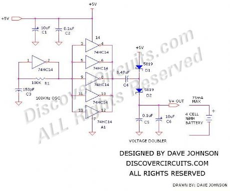
View full Circuit Diagram | Comments | Reading(930)
MOBILE CELLPHONE CHARGERS
Published:2012/11/8 1:09:00 Author:muriel | Keyword: MOBILE CELLPHONE, CHARGERS
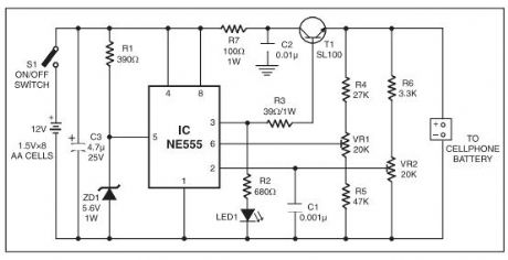
View full Circuit Diagram | Comments | Reading(1231)
| Pages:38/291 At 202122232425262728293031323334353637383940Under 20 |
Circuit Categories
power supply circuit
Amplifier Circuit
Basic Circuit
LED and Light Circuit
Sensor Circuit
Signal Processing
Electrical Equipment Circuit
Control Circuit
Remote Control Circuit
A/D-D/A Converter Circuit
Audio Circuit
Measuring and Test Circuit
Communication Circuit
Computer-Related Circuit
555 Circuit
Automotive Circuit
Repairing Circuit