
power supply circuit
Index 22
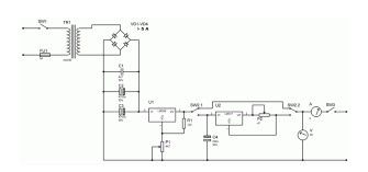
600 Watt Uninterruptible Power Supply
Published:2013/3/22 3:38:00 Author:Ecco | Keyword: 600 Watt, Uninterruptible Power Supply
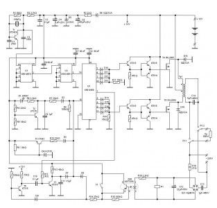
The schematic in figur is the circuit of 600W UPS. Stay powered and radio during a power failure. Output frequency – 50 Hz, Power Consumption 600 Watts, the shape of the output signal – sinusoidal, the efficiency – 98%. The device contains an auto power off at the mains, followed by automatic switch-off with the appearance of tension.
(View)
View full Circuit Diagram | Comments | Reading(4432)
Simple 12 Volt to 9 Volt DC-DC Converter
Published:2013/3/22 3:34:00 Author:Ecco | Keyword: 12 Volt to 9 Volt, DC-DC Converter
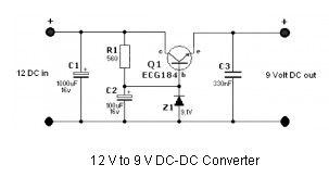
This DC-DC Converter schematic diagram is very simple with few components, making it easy to build. It can convert 9 volt DC voltage from 12 VDC source.
To obtain a much more accurate output voltage, change zener Z1 using 10V and resistor R1 with a 1 Kohm Variable resistor. A heatsink for Q1 is recommended. Very simple circuit to be able to power your 9 volt electronic equipment and some other stuff.
(View)
View full Circuit Diagram | Comments | Reading(3436)
200W ATX Power Supply Circuit
Published:2013/3/22 3:33:00 Author:Ecco | Keyword: 200W , ATX Power Supply
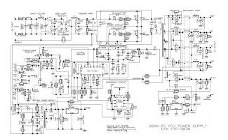
This an ATX power supply circuit diagram, dedicated for personal computer, but you may use this power supply for other electronic devices. The circuit is built using chip TL494, and will give you approximately 200W. It use push-pull transistor circuit with regulation of output voltage.
Line voltage goes via input filter circuit (C1, R1, T1, C4, T5) to the bridge rectifier. When voltage is switched from 230V to 115V, then rectifier works like a doubler. Varistors Z1 and Z2 have overvoltage secure function on the line input.
(View)
View full Circuit Diagram | Comments | Reading(3776)
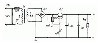
13.8V / 10A DC Regulator Circuit
Published:2013/3/22 3:32:00 Author:Ecco | Keyword: 13.8V / 10A, DC Regulator
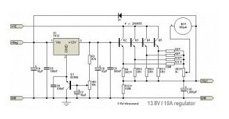
This is a dc regulator circuit which will give output voltage of 13.8V with current output about 10A. The circuit use 4 pieces of power transistor 2N3055 to boost the electric current, to make the circuit capable to deliver 10A current output. It also use IC regulator 7812, change the IC type will give different output voltage value.
(View)
View full Circuit Diagram | Comments | Reading(2869)
Convert PC Power Supply to Bench Power Supply
Published:2013/3/22 3:32:00 Author:Ecco | Keyword: Convert PC Power Supply, Bench Power Supply
View full Circuit Diagram | Comments | Reading(1371)
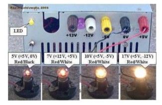
ATX Power Supply Pinout
Published:2013/3/22 3:31:00 Author:Ecco | Keyword: ATX Power Supply
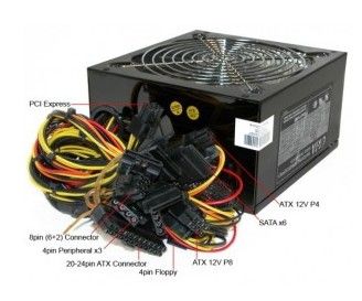
The ATX power supply generates three main voltage outputs that are: +3.3 V ; +5 V ; and +12 V. Low-power −12 V and +5 VSB (standby) supplies are also generated by this power supply. The −5 V output was originally needed since it was supplied on the ISA bus, however it became obsolete with the removal of the ISA bus in modern day PCs and has been removed in later versions of the standard ATX power supply.
(View)
View full Circuit Diagram | Comments | Reading(1715)
High-voltage power supply circuit for fluorescent light
Published:2013/3/22 3:30:00 Author:Ecco | Keyword: High-voltage , power supply , fluorescent light
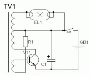
The following figure shows a diagram of power fluorescent lights to a normal battery. It is very convenient when you can not use the grid.
(View)
View full Circuit Diagram | Comments | Reading(1202)
Transformerless power supply FET
Published:2013/3/22 3:29:00 Author:Ecco | Keyword: Transformerless power supply , FET
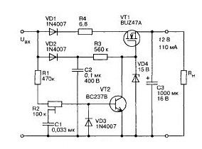

The circuit shows a diagram of a simple transformerless power supply for transistor BUZ41A. Through the inclusion of the common-drain transistor VT1 NW capacitor charging to a voltage of about 3 smaller than the zener voltage of VD4. An alternating voltage with a phase shift, determined by the capacity of the capacitor C1, transistor opens VT2, which stops the charge capacitor NW at the beginning of each positive half-wave supply voltage.
(View)
View full Circuit Diagram | Comments | Reading(2964)
Simple Variable Power Supply 1.5 – 30V, 5A
Published:2013/3/22 3:28:00 Author:Ecco | Keyword: Simple Variable Power Supply , 1.5 – 30V, 5A
The power supply is based on two chips and in addition they contain only a few discrete components. In this regard, it is easy to manufacture and configuration. At the same time, the power supply provides a high level indicators, such as the smooth adjustment of the voltage in the large range, low coefficient of fluctuation, the output current up to 5A with the ability to stabilize the current, high reliability. Also, the power supply has short circuit protection.
(View)
View full Circuit Diagram | Comments | Reading(2071)
Simple power supply 5V, 0.5A
Published:2013/3/22 3:27:00 Author:Ecco | Keyword: Simple power supply, 5V, 0.5A
The power supply is designed to supply a stabilized 5V various digital devices with current consumption up to 0.5 A. The transformer T1 is made on the magnetic core SHL20H32.The network contains 1650 turns of PEV-1 d = 0,1 mm, coil II – 55 turns of PEV-1 d = 0,47.In general, for the power supply can use a suitable transformer ready 7W, which provides for winding II AC 8 … 10 V at a current of 500 mA.Regulating transistor VT2 is mounted on the L-shaped dural plate 50×50 and 2 mm thick.
(View)
View full Circuit Diagram | Comments | Reading(1002)
Transformerless power supply from 220V with LM2575
Published:2013/3/22 3:26:00 Author:Ecco | Keyword: Transformerless, power supply, 220V
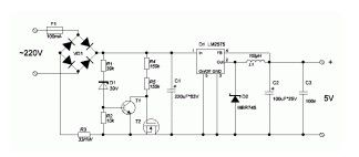
Is often requiredtosupply electricityto theconsumerlowvoltage 220V. Youcanusean externaladapter- butit’s bad,andtoreduce the size ofthe devicerequires apower supplylocatedin the device.
This 5v power supply used LM2995 to the convertercircuitwhichcan be connected directly to220V. Todo this, ACconvertedto DCvoltageacross the diodebridgeVD1, andthenloweredto40V. Above 40Vwe should notuse it, due to the factthat theLM2995maximum input voltagemustnotexceed45V.
Transistors T1 and T2 form a pulsating stress amplitude up to 40V, which depends on the zener diode D1. This pulsating voltage is applied to the capacitor C1, which is slightly smoothed. Next on the chip down-converter output voltage is stabilized, defined applied chips : so for LM2575-5 5V it will be equal. Schottky diode D2, L1, C2 and C3 are the standard strapping of the chip.
(View)
View full Circuit Diagram | Comments | Reading(3666)
Step up DC / DC Converter with LT1615
Published:2013/3/22 3:25:00 Author:Ecco | Keyword: Step up , DC / DC Converter
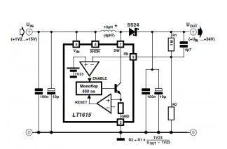
Interesting DC / DC converter Linear Technology has presented the company, this chip is the boost converters that allow you to get the maximum voltage in 34B with the input voltage from 1.2V to 15V. It comes in a compact package of 5 pin SOT23, while for work requiring minimal external circuitry. These chips can be used, for example, a high voltage for the LCD screen or for the varicap.
(View)
View full Circuit Diagram | Comments | Reading(1833)
DC Voltage Doubler Circuit +12V to +24V using LM2586
Published:2013/3/22 3:24:00 Author:Ecco | Keyword: DC Voltage Doubler, +12V to +24V
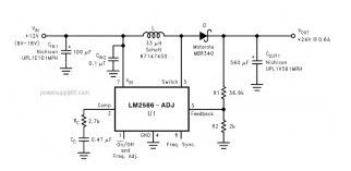
This is the DC voltage doubler circuit which build based National IC LM2586. The circuit will doubling the input voltage of 12VDC to become 24VDC. Heatsink is required for this circuit.
The LM2586 is a monolithic integrated circuits specifically designed for flyback, step-up (boost), and forward converter applications. The device is available in 4 different output voltage versions: 3.3V, 5.0V, 12V, and adjustable.
(View)
View full Circuit Diagram | Comments | Reading(2446)
Additional Power Supply for USB Devices
Published:2013/3/22 3:24:00 Author:Ecco | Keyword: Additional Power Supply , USB Devices
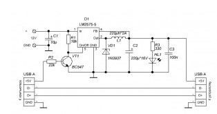
Much the use of USB devices today, sometimes cause lack of power problem. How to know the maximum current that can be obtained from a single USB connector is limited to 500 mA. If your device requires more current, then it must involve an additional one USB connector, which maybe not available. This problem can be solved by an additional instrument to use an external unregulated power and convert it to 5 Volt.
You can use two different approaches. You can use two different approaches. the first and perhaps easiest – is to use a simple linear regulator, but this raises other problems – wasteful spending power, but you can go the other way and use a pulse transformer, which is more economical.
Note : The basis of the converter is a PWM controller based on integrated circuits LM 2575-5, having the output of 5 volts with a current up to 1A. To enable / disable the converter uses pin 5 On / Off , controlled transistor VT 1.
(View)
View full Circuit Diagram | Comments | Reading(1307)
Voltage Converter from 1.5V to 3V
Published:2013/3/22 3:19:00 Author:Ecco | Keyword: Voltage Converter , 1.5V to 3V
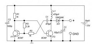
A simple scheme to generate the inverter voltage from 1.5V to 3V can be made on the basis of slightly modified the well-known multivibrator. Under these denominations in the scheme of the frequency converter is approximately 130 kHz. Inductance value can be calculated or chosen experimentally. But you can simply adjust the frequency of the converter to produce maximum output voltage. Schottky diode VD1 can be replaced by any other similar characteristics.
For further stabilization of the output voltage can be applied to the zener voltage of 3V – 3.3V. This scheme can be used to power a LED or low power devices based on the microcontroller, for example, MSP430.
(View)
View full Circuit Diagram | Comments | Reading(2213)
Mains AC / DC Converter with SR03x
Published:2013/3/22 3:14:00 Author:Ecco | Keyword: Mains AC / DC Converter
This is another Transformerless power supply. IC voltage regulators for SR03x made by Supertex is connect directly to main voltage and get the output voltage to 3.3V and 5V chip for SR036 SR037 to 30mA output current. To use this chip is not necessary to use step-down transformer or coil. Rectified input voltage to the diode bridge diodes D1 – D4 (figure point a) is input circuits IC1 SR03x.
(View)
View full Circuit Diagram | Comments | Reading(999)
Low Power Bipolar Stabilizer
Published:2013/3/22 3:13:00 Author:Ecco | Keyword: Low Power, Bipolar Stabilizer
The stabilizer is made on the integrated circuit KR142EN6. IC is a bipolar voltage regulator with an output voltage of + / -15 V. Maximum load current is 200 mA. Enough to supply a pre-amplifier or the early stages of the power amplifier.Diode bridge – any of a series of KTS407, KTS405, KTS402.Transformer with two secondary windings, the voltage on each – 16 Volt.
(View)
View full Circuit Diagram | Comments | Reading(803)
6.8 Volt Transformerless Power Supply
Published:2013/3/22 3:13:00 Author:Ecco | Keyword: 6.8 Volt, Transformerless Power Supply
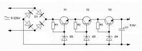

The scheme is designed for voltage and current of 6.8 V 300mA. The voltage can be changed by replacing the Zener D4 and, if necessary, D3. A setting on the radiators of transistors can be increased and the load current.Diode bridge – any, is nice and a reverse voltage of at least 400 volts. By the way, we can recall the ancient and diode D226B, once terribly popular.
(View)
View full Circuit Diagram | Comments | Reading(1355)
1.5V-25V Power Supply with Preregulator
Published:2013/3/22 3:12:00 Author:Ecco | Keyword: 1.5V-25V , Power Supply , Preregulator
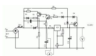
This circuit using KR142EN12 (analog – LM317 ) ic regulator that can handle load currents up to 2 amperes. For higher currents can be used IC LT1083/84/85 that each can handle currents 7/5/3A. 2000uF capacitor C3 is selected from the calculation of the current 1 Ampere. Resistor R9 is used as a current sensor to an ammeter.
In fact, not all of the thyristor passes the half-wave rectified voltage, and some of them, depending on the output voltage and load current. This can significantly reduce the power dissipated in the regulating element, especially at low output voltages and currents.
(View)
View full Circuit Diagram | Comments | Reading(1510)
70 W Switching Power supply with KA2S0880 IC
Published:2013/3/22 3:11:00 Author:Ecco | Keyword: 70 W, Switching Power supply
The schematic shows the power supply capacity of 70W stereo amplifier Power converter is built on a chip KA2S0880, which includes all the necessary components to build the primary of the power supply. This chip is very stable in operation and has all the necessary protections.
(View)
View full Circuit Diagram | Comments | Reading(1883)
| Pages:22/291 At 202122232425262728293031323334353637383940Under 20 |
Circuit Categories
power supply circuit
Amplifier Circuit
Basic Circuit
LED and Light Circuit
Sensor Circuit
Signal Processing
Electrical Equipment Circuit
Control Circuit
Remote Control Circuit
A/D-D/A Converter Circuit
Audio Circuit
Measuring and Test Circuit
Communication Circuit
Computer-Related Circuit
555 Circuit
Automotive Circuit
Repairing Circuit