
Amplifier Circuit
Index 204
The circuit diagram of preamplifier serving the electric motor drive circuit
Published:2011/6/1 22:31:00 Author:leo | Keyword: The circuit diagram of preamplifier serving the electric motor drive circuit, MC1437
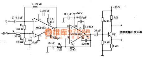
Picture 1 shows a preamplifier that serves the electric motor drive circuit. In this circuit, 90° phase shift adopts differential coefficient circuit with operational amplifier MC1437 (1). It is connected to in-phase amplifier MC1437 (2) with the voltage plus of 40 dB. Feedback resistance R1 and input capacitance C1 can make up of differential circuit. R3 and R4 are used to set DC operating point of operational amplifier. And the operating point is set in the 1/2 of the voltage of power supply. The gain of differential circuit increases by the frequency. Therefore, the circuit may develop into high-frequency section and it needs to limit bandwidth. The single-ended output of MC1437 (2) passes VT1 and becomes two ways signals in order to drive sh-pull (PP) output amplifier. (View)
View full Circuit Diagram | Comments | Reading(697)
The push-pull power amplifier circuit formed by MOSFET
Published:2011/6/9 3:02:00 Author:leo | Keyword: The push-pull power amplifier circuit formed by MOSFET
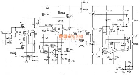
The picture 1 shows a push-pull power amplifier circuit formed by MOSFET. VT1 and VT2 form the propel circuit, which uses transformer T1 to get the same output value but different polarity signals. And the signals are driven separately by the power output ports formed by VT3 and VT4 (VT5 and VT6). In order to increase output power, when the operating power is 1 kHz, the minimum distortion is 0.25%. The voltage gain of median frequency period is 31.5 dB.When voltage gain is -3dB, the bandwidth is narrow, which is 11 kHz to 16.8 kHz. When input port is short or cut off, noise voltage is 0.22 mV. So it has excellent performance.
(View)
View full Circuit Diagram | Comments | Reading(2944)
The audio frequency power amplifier with 40W to 60 W output power and formed by MOSFET
Published:2011/6/10 21:09:00 Author:leo | Keyword: The audio frequency power amplifier with 40W to 60 W output power and formed by MOSFET
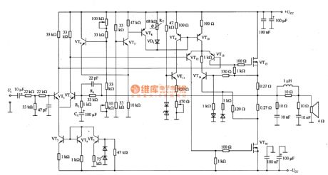
The picture 1 shows a audio frequency power amplifier circuit diagram. It is made up of MOSFET with the output power of 40 to 160 W. In this circuit, the DC current feedback between power output stages to preamplifier stage is decided by the value of R1, while the AC current feedback is decided by the resistance value and capability of C1. The basic amplifying circuit is formed by series connecting the two stages differential amplifiers of VT1, VT2 and VT12 and VT13. The operating point of VT1 and VT2 is decided by constant current circuit VT3, while it is the same condition to VT12 and VT13. VT6, VT7, VT8 and thermistor RT form temperature protection circuit. VT14 forms the over current protection circuit. When the current value of output power MOSFET is stronger than the set value, VT14 is connected while VT12 and VT13 push the current to be weakless, and VT15 and VT16 is cut off. Therefore, all processes reach the final result of protecting the MOSFET. (View)
View full Circuit Diagram | Comments | Reading(3345)
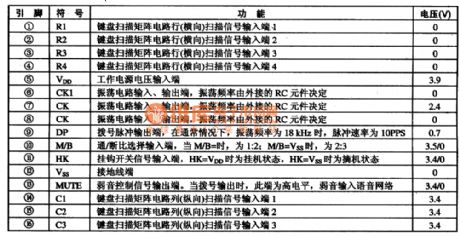
M62438-dual channel SUR solution circuit
Published:2011/6/10 21:24:00 Author:leo | Keyword: M62438-dual channel SUR solution circuit
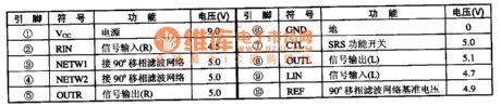
M62438 is the integrated circuit of the dual-channel analog SUR solution, which is widely used in audio devices and audio system of the advanced big screen color TV. It is produced by Mitsubishi in Japan.
1.Function features:M62438 contains two 90 angel phase-moving filter system, SRS function switch control circuit, basic power supply circuit of 90 angle phase-moving filter system, and other related circuits.
2.Pin function and dataM62438 adopts 10-pin package methods. Functions of all pins and related data are shown in the picture. (View)
View full Circuit Diagram | Comments | Reading(676)
The microcomputer dialing circuit UM-915-3
Published:2011/6/10 21:32:00 Author:leo | Keyword: The microcomputer dialing circuit UM-915-3
UM-915-3 is a microcomputer dialing circuit which is applied in all kinds of telephone.
1.Function features:Integrated circuit UM-915-3 contains a pulse dialing signal processing circuit and key switch code circuit and other circuits.
2.Pin function:Functions of all pins and related data of UM-915-3 are shown in the picture. (View)
View full Circuit Diagram | Comments | Reading(653)
the circuit of zero-delay RS-485 port
Published:2011/5/27 7:22:00 Author:Ariel Wang | Keyword: zero-delay, RS-485, port
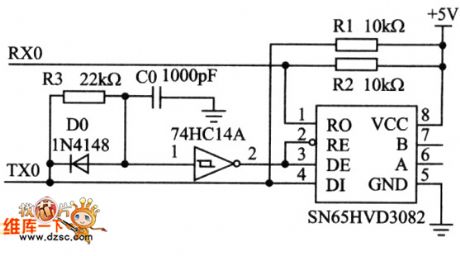
The circuit of zero-delay RS-485 port is as the chart below: (View)
View full Circuit Diagram | Comments | Reading(2739)
the circuit of ADS7824 parallel port
Published:2011/5/26 23:30:00 Author:Ariel Wang | Keyword: ADS7824, parallel port
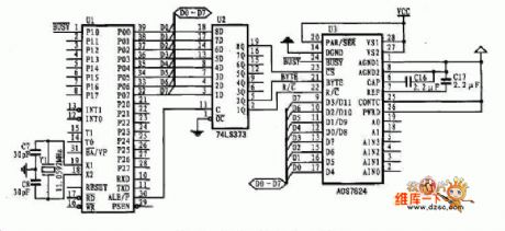
The circuit of ADS7824 parallel port is as below:
(View)
View full Circuit Diagram | Comments | Reading(605)
the circuit of MSM6822 applied
Published:2011/5/26 23:24:00 Author:Ariel Wang | Keyword: MSM6822 applied
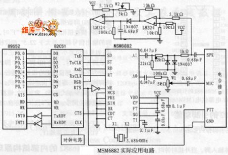
The circuit of MSM6822 applied is as below:
(View)
View full Circuit Diagram | Comments | Reading(586)
The power amplifying circuit formed by LM377 and others
Published:2011/6/1 22:41:00 Author:leo | Keyword: The power amplifying circuit formed by LM377 and others, LM377
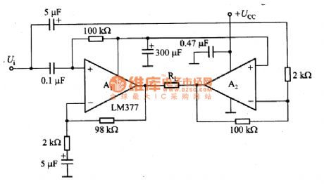
Picture 1 is a power amplifying circuit formed by LM377 and others. LC377 is a integrated circuit which has two in-die power amplifiers. If making the two power amplifiers connecting as electronic bridge, it can supply double power in valve to floating land negative load RL. Negative load RL can be servo motor or speaker. A1 and DC output port has the same electric potential, so it can not be connected to the stop capacitor with large capability.
When the negative load is 8 to 16 Ω, the response frequency of the circuit is 20Hz-160 KHz. When output power is 4W, the distortion of middle frequency is 0.1%. And when output power is 50mW, the distortion of middle frequency is 0.5%. (View)
View full Circuit Diagram | Comments | Reading(1445)
The current detection circuit formed by FET
Published:2011/6/8 21:00:00 Author:leo | Keyword: The current detection circuit formed by FET
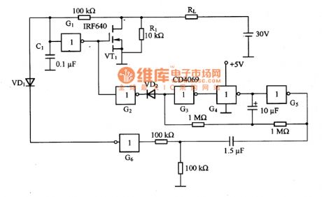
The picture shows a current detection circuit formed by FET and others. In this circuit, VT1 is the switch. When VT1 is saturated, it will act as current detection resistance.When the current flowing through VT1 is too heavy, the voltage between source and drain will increase. Then the inverter G1 will detect the voltage. And this can make the grid voltage of VT1 lower while the drain voltage increases, which make the whole circuit break away from the steady condition. Under this situation, almost no current flows through load RL. Therefore, VT1 can be regarded as fusible link. Because when the current passing through VT1 is too heavy, VT1 will be burned out and the current flowing through load RL is zero.
(View)
View full Circuit Diagram | Comments | Reading(718)
The high-end current monitor circuit formed by AD202
Published:2011/6/8 21:07:00 Author:leo | Keyword: The high-end current monitor circuit formed by AD202, AD202
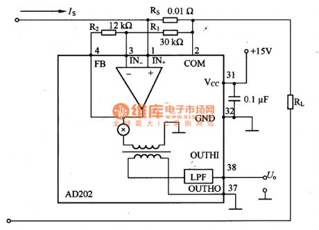
What the picture shows is a high-end current monitor circuit formed by AD202 and others. AD202 is a kind of amplifier that has inner transformer isolation. In this circuit, the maximum valve of power supply voltage is decided by voltage resistance of AD202. The voltage resistance of AD202 is 750 V which can meet the practical application needs. (View)
View full Circuit Diagram | Comments | Reading(1058)
The amplifer circuit formed by LM121 and used in device
Published:2011/6/8 21:08:00 Author:leo | Keyword: The amplifer circuit formed by LM121 and used in device, LM121
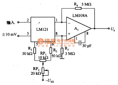
Picture 1 is an amplifier used in device. It is made up of LM121 and others. LM121 changes the differential input voltage into differential output voltage to drive the backdrop operating amplifier A1. A1 can form current-voltage converting circuit which change differential input to output. R1, R2 and RP1 are used to set the working current of LM 121 and regulate the imbalance current(voltage) of the circuit. While RP2 is used to regulate gain. They do not influence each other. The limited input voltage of LM121 is ±10mV, which can form higher common mode rejection ratio (120dB) and low drifting device amplifier. (View)
View full Circuit Diagram | Comments | Reading(917)
The high-end current monitor circuit formed by OP184
Published:2011/6/8 21:12:00 Author:leo | Keyword: The high-end current monitor circuit formed by OP184, 2SA970, OP184, MOSFET
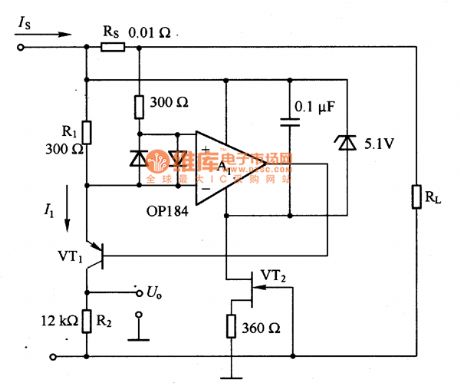
The picture shows a high-end current monitor circuit formed by OP184. In this circuit, A1 adopts OP184 operating amplifier. VT1 adopts 2SA970 transistor. When Is comes close to OA, the collector cutoff current of VT1 is the main factor that causes differences. When VT1 selects P channel JFET, it can improve detection precision. Now JFET with high pressure resistance is rare. So P channel MOSFET can be used instead of it. Using high degree accuracy resistance will also improve the detecting accuracy. (View)
View full Circuit Diagram | Comments | Reading(1762)
The circuit diagram of amplier formed by 2SJ114
Published:2011/6/8 21:34:00 Author:leo | Keyword: The circuit diagram of amplier formed by 2SJ114, 2SJ114
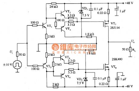
The picture 1 shows a amplifier circuit formed by 2SJ114.It can amplify square wave signal of ±l0V to ±48V. This circuit adopts P channel and N channel power MOSFET(VT7 and VT8) to form switch circuit. And the switch circuit is symmetry in the face and the below sides, so it can output dual polarity voltage. Due to the operating mode of VT7 and VT8 (the same power source), it needs to use VT3 to VT6 transistors to form the low resistance drive circuit in order to improve the response speed of gates. (View)
View full Circuit Diagram | Comments | Reading(3490)
The high-end current monitor circuit formed by INA168
Published:2011/6/8 21:50:00 Author:leo | Keyword: The high-end current monitor circuit formed by INA168, INA168
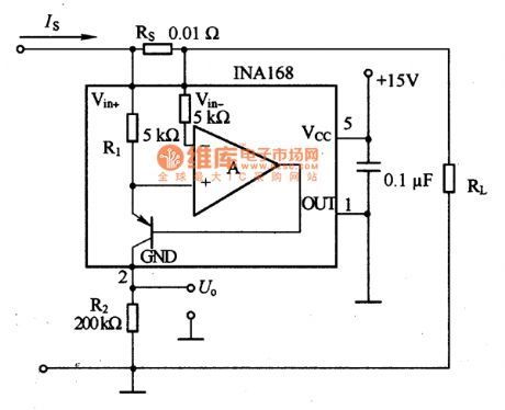
What the picture shows is a high-end current monitor circuit formed by INA168. When detecting the changing current of the power supply, loop wire is connected to the ground by the side. Sometimes, the enclosure and rock can not be connected to diverge resistance, it needs to connect Rs to the plus terminal of power supply to test the voltage difference generating by the current passing through Rs in order to detect the current passed through.
In this circuit, INA168 is specailly used to detect the current. The followings are some parameters of it: The voltage of power supply is 30 to 60 V. The maximum current it can detect is 10 A. When the current value is 10 A, the output detecting voltage should be 4 V. When the detecting voltage of power supply is low, it needs to use operating amplifier to form differential amplifier. But this circuit is suitable for the application under high power supply. (View)
View full Circuit Diagram | Comments | Reading(1972)
The high-speed absolute value amplifier circuit diagram
Published:2011/6/8 22:01:00 Author:leo | Keyword: The high-speed absolute value amplifier circuit diagram, LM318, HA2525

The picture 1 shows a high-speed absolute value amplifier circuit. The operating amplifier and diode form the ideal diode circuit which is used to detect communication signals. However, in the ideal diode circuit, rectified input voltage gives an effect directly to the frequency of operating amplifier and high frequency is limited. High speed operating amplifier, such as LM318, HA2525, μA715 and so on, can ensure an over 100kZ operating frequency. Operational Amplifier should be selected in the high-speed absolute value amplifier circuit. In this circuit, A1 uses HA2526 operational amplifier and also LM318. But the cut-off distortion of diode affects the high frequency operating, therefore, it takes VT1 and VT2 to form constant current source in this circuit. (View)
View full Circuit Diagram | Comments | Reading(1607)
The low-end current monitor circuit formed by AD8551
Published:2011/6/9 2:47:00 Author:leo | Keyword: The low-end current monitor circuit formed by AD8551, AD8551

The picture shows a low-end current monitor circuit formed by AD8551, which is used to detect the motor current or charging current. When detecting the current of the motor or rechargeable battery, high-end monitor is frequently used, which is usually used to detect the power sourcing current.
In this circuit, A1 adopts highly accurate operating amplifier AD8551 which uses +2.7 to +5V signal power source to operate. (View)
View full Circuit Diagram | Comments | Reading(1915)
The high input resistance amplifier circuit formed by FET
Published:2011/6/8 22:13:00 Author:leo | Keyword: The high input resistance amplifier circuit formed by FET
The picture 1 shows a high input resistance amplifier circuit. The picture 1(a) is the sourcing follower circuit formed by FET. The voltage gain of the follower: Av=gmRL/(l+gmRL); gm is mutual conductance; RL is sourcing load resistance. If Ac needs to be near 1, FET with bigger gm value is needed with the resistance value RL as big as possible. In order to increase the RL value, constant sourcing current formed by VT2 is adopted.
The picture1 (b) is the high input resistance circuit formed by FET. R1 is the grid offset deciding resistance. The current pass through R1 is usually very small. So the resistance is super high in the circuit.The Picture1 (c) is the circuit connected to operational amplifier. It is made up of two simple FET. RP1 is used to investigate the offset voltage. (View)
View full Circuit Diagram | Comments | Reading(1697)
Overvoltage Detection Circuit Diagram formed by LTC1541 and Others
Published:2011/5/21 21:34:00 Author:leo | Keyword: Overvoltage Detection Circuit Diagram formed by LTC1541 and Others, 1N4005, ZTX458, 100K, 300K, 600V, LTC1541, 240V
As the picture shows, this is a overvoltage detection circuit. It is applied to detect the overvoltage in any power supply circuit with a detection scale from 3 V to hundreds of voltage. Besides, it can also be used to lock detect the voltage which can detect 30μs transient overvoltage peak pulse. Under the common condition, the current consumption of this circuit will be under 25μA. So it is the best voltage control circuit in the battery power supply system.
LTC1541 applied in this circuit is a kind of integrated circuit which contains a comparator A1 that has a small power compensation, operating amplifier A2 as well as UREF with the referred voltage of 1.20 V. This circuit demands a maximum of 13μA. (View)
View full Circuit Diagram | Comments | Reading(681)
Digital Meter Panel Circuit Diagram made up of PIC16C711 and Others
Published:2011/5/20 22:13:00 Author:leo | Keyword: Digital Meter Panel Circuit Diagram made up of PIC16C711 and Others, PIC16C711
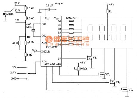
As the picture shows, this is a electrical digital meter panel circuit. As a 8 bits A/D converter, PIC16C711 has two input ports. Among them, AD0 is voltage input port and AD1 is scale selecting input port. If AD1 is connected to ground, it will show a scale of 0.00 V to 5.10 V with resolution of 20 mV. If AD1 is connected to 2.5V voltage, it will show a scale of 00.00 V to 12.75 V with the resolution of 50 mV. If AD1 is connected to 5 V, it will show a scale of 00.0 V to 25. 5 V and the resolution will be 100 mV. Under the common condition, PIC16C711 display accuracy is ±1/2LSB. It can drive four seven-port LED at the same time and only one LED can be lighted at one time. The input voltages of PIC16C711 are 5 V, 12 V and 25 V. (View)
View full Circuit Diagram | Comments | Reading(5195)
| Pages:204/250 At 20201202203204205206207208209210211212213214215216217218219220Under 20 |
Circuit Categories
power supply circuit
Amplifier Circuit
Basic Circuit
LED and Light Circuit
Sensor Circuit
Signal Processing
Electrical Equipment Circuit
Control Circuit
Remote Control Circuit
A/D-D/A Converter Circuit
Audio Circuit
Measuring and Test Circuit
Communication Circuit
Computer-Related Circuit
555 Circuit
Automotive Circuit
Repairing Circuit