
Amplifier Circuit
Index 216
Analog isolation circuit
Published:2011/5/29 22:07:00 Author:chopper | Keyword: Analog, isolation
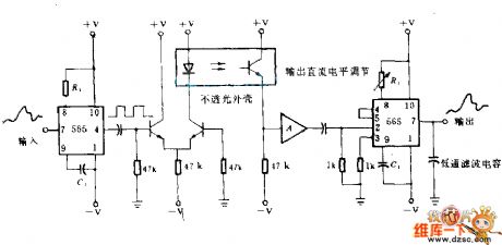
This circuit is a FM transmission system which uses light as media.The transmitter uses 565 phase-locked loop as voltage controlled oscillator,making the LED of optoelectronic isolator flash at a rate that is proportional to input voltage.The driving amplifier of photoduodiode is of enough gain to add 200mV(peak-peak) signal to the input end of recipient 565.Recipient 565 is acted as a frequency modulation detector and reproduces the signal which is imported to the transmitter.The power source is between ±6 and ±12V.
(View)
View full Circuit Diagram | Comments | Reading(2337)
The optoelectronic isolation circuit between TTL and relay
Published:2011/5/28 0:43:00 Author:chopper | Keyword: TTL, relay, optoelectronic isolation circuit
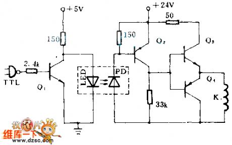
In this circuit,it uses photocoupler to make the circuit between TTL and relay gain the isolation of 100GΩ,and eliminates the effect to TTL circuit from noise of relay as well as spike voltage.When the input signal of TTL is high,Q1 is conducted,and LED has no current.And there is no light incidenting to detectors.At this time,photoelectric diode has the bigest resistance value of 5GΩ.Therefore,Q2 is inconductive,so is Q3.Thus,no current passes through the coil of relay.
(View)
View full Circuit Diagram | Comments | Reading(1205)
the Integral reset circuit of improved I
Published:2011/5/30 7:14:00 Author:Ariel Wang | Keyword: Integral, reset, improved I

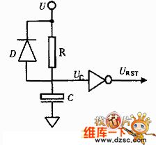

From below we can see that the time constant of discharge circuit usually far less than of charge circuit.At this time,the unreliable phenomenon of power on reset caused by switch on and off can be controlled . As the time constant of discharge is too short,it reduces the insensitiveness of voltage fluctuation to power-supply when the reset circuit is at work.
(View)
View full Circuit Diagram | Comments | Reading(737)
the circuit of hardware in SD1077 singlechip system
Published:2011/5/29 23:15:00 Author:Ariel Wang | Keyword: hardware, singlechip system
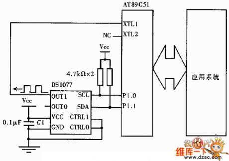
The circuit of hardware in SD1077 singlechip system is as the chart below:
(View)
View full Circuit Diagram | Comments | Reading(541)
the reset circuit of MAX706P
Published:2011/5/29 23:15:00 Author:Ariel Wang | Keyword: reset
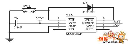
The reset circuit of MAX706P is as the chart below:
(View)
View full Circuit Diagram | Comments | Reading(520)
the circuit of static digital display
Published:2011/5/29 23:17:00 Author:Ariel Wang | Keyword: static , digital, display
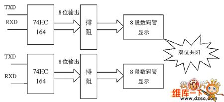
It can be divided into static display and dynamic display as there are two ways of display.Here what we talked about is static display.It is two-bits static digital display.Its main function is displaying the serial number of LED light which is on.If L1 light is on,digital tube will display 11.If L2 is on,digital tube will display 22,ect.The design of the circuit is composed of two 8-bits shift register (74HC164), two 8-sections LEB digital tube( Common anode) and two 8×330Ω exclusion .
(View)
View full Circuit Diagram | Comments | Reading(565)
the joint circuit of ADS7805 and TMS320F206
Published:2011/5/29 23:18:00 Author:Ariel Wang | Keyword: joint
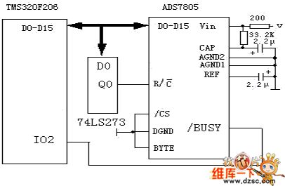
The 16-bit fixed point DSP TMS320F206 of T1 company is low power device.It adopts improved Harvard structure .It has one procedure base line,3 data base lines,assembly lines and so on.When TMS320F206 externally connects the 16MHZ crystal oscillator ,and the control mode of working clock is ×1,you can connect /CS pin to DSP's /RD signal pin.But in order to reduce the controlling line,you can reduce /CS's pin to low level .You can connect R/C's pin to /RD's signal pin and you can connct R/C's pin to DSP expanding output port.But /BUSY signal can only be connected to common input port.For example,DSP's IO port,expanding chip 74LS244's input port,ect.
(View)
View full Circuit Diagram | Comments | Reading(615)
the joint circuit of DSP and 8237
Published:2011/5/29 23:19:00 Author:Ariel Wang | Keyword: joint, DSP

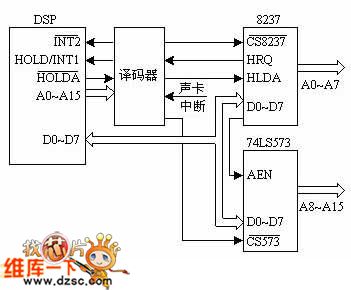
The circuit as the chart below provides DMA service signal from 4 channels' peripheral demands.And 8237 has AEN pin.It can satisfy all requests of chart 1.So it reallizes the interface between DSP and the sound card.In actual work,we based on the situation of usage of the sound card in PC to set up whether 8237's DREQ1 or DACK1 can be the play passage,whether 8237's DREQ3 or DACK3 can be the collecting passage,whether the break application signal IRQ7 goes through GAL16V8 becoming reversed with DSP'spin or not.
(View)
View full Circuit Diagram | Comments | Reading(617)
the AD9850 circuit
Published:2011/5/29 23:30:00 Author:Ariel Wang | Keyword: circuit
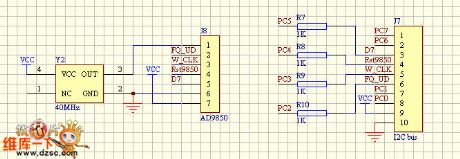
The AD9850 circuit is as the chart below:
(View)
View full Circuit Diagram | Comments | Reading(619)
the independent oscillator divider circuit of watchdog delicated chip TPS3823
Published:2011/5/30 10:29:00 Author:Ariel Wang | Keyword: independent, oscillator divider , watchdog, delicated chip
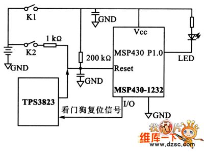
①Because the clock of the watchdog is dependent,the counting clock and the system belong to the same frequency division link.The watchdog won't operate effectively when the system have some problems.②The clock can use software to set up.When the setting up is failed,the clock may fail as well. Without clock,watchdog can't work well.③Some watchdog need software to set up and start.So when the start fails and initialization unactivated,CPU might jump to random code.It may stop the watchdog.Theoretically,the design has the unreasonable part.Based on the analysis above,we adopt off chip watchdog using dedicated chip TPS3823.The experimental circuit is seen as below:
(View)
View full Circuit Diagram | Comments | Reading(787)
the reset circuit of improved comparator
Published:2011/5/28 18:22:00 Author:Ariel Wang | Keyword: reset, improved, comparator
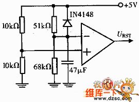
The reset circuit of improved comparator is as the chart below:
(View)
View full Circuit Diagram | Comments | Reading(569)
the compound circuit of basic comparator
Published:2011/5/28 18:26:00 Author:Ariel Wang | Keyword: compound circuit, basic, comparator
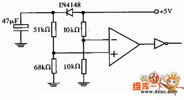
The compound circuit of basic comparator is as the chart below:
(View)
View full Circuit Diagram | Comments | Reading(621)
the circuit of power supply isolation
Published:2011/5/28 18:34:00 Author:Ariel Wang | Keyword: power supply, isolation
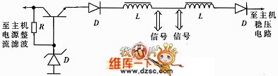
The circuit of power supply isolation is as the chart below:
(View)
View full Circuit Diagram | Comments | Reading(445)
Measuring Bridge Amplifier Circuit
Published:2011/5/21 20:30:00 Author:Robert | Keyword: Measuring Bridge, Amplifier
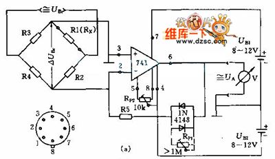
In the circuit (a) the measuring bridge is made up by R1~R4 resistances. The output voltage URr can be DC or AC voltage (maximum 100kHz). If it is AC voltage it can use the coupling capacitor (picture b). And it can use high resistance in these two cases.
(View)
View full Circuit Diagram | Comments | Reading(587)
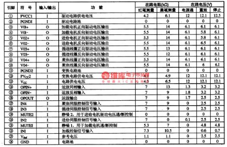
AN8812K-the integrated servo-driven circuit
Published:2011/5/18 0:17:00 Author:Borg | Keyword: servo-driven, integrated
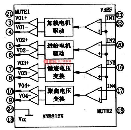
AN8812K is an integrated servo-driven circuit produced by Panasonic Corp., Japan, which is used in DVD core as the laser head servo driver.1.the internal circuitAN8812K contains 4-channel servo driven circuits, whose internal circuit is listed in Figure 1.
Figure 1 the internal circuit of AN8812K2.pin functions and dataAN8812K is in 24-lead dual line package, whose pin functions and data are listed in Table 1, the data come from tests on TCL DVD-250O.
(View)
View full Circuit Diagram | Comments | Reading(661)
AN8481SQ-the integrated circuit of 3-spindle motor and loading motor drives
Published:2011/5/18 4:08:00 Author:Borg | Keyword: integrated circuit, motor drives
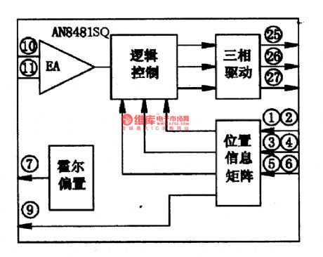
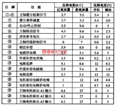
1.function featuresAN8481SQ is supposed to convert the spindle servo error control signals into 3-phase drive voltages to drive the motor, whose internal circuit is shown is Figure 1.
2.pin functions and dataAN8481SQ has a function of overheat protection, which is in flat 28-lead package with cooling fins. It is used in GD2O0l DVD player of Hitachi, whose pin functions and data are listed in Table 1. In the table, the pins of (21), (23) and (24) are empty, (14) and (16) are earth terminals, (28) is the earth terminal of the drive circuit.
(View)
View full Circuit Diagram | Comments | Reading(516)
DC photoelectric switch circuit
Published:2011/5/24 2:05:00 Author:John | Keyword: DC photoelectric switch
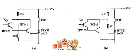
Phototransistor BPX25 in Figure (a) stops where there is no light irradiation. So the no base current of transistor BC141 is off. Otherwise, the transistor opens to trigger thyristor to conduct. Then, voltage is on the negative cut-off side.
The Figure (B) shows the opposite situation. When light shines into the phototransistor, the transistor BC141 conducts to cut-off the thyristor. Then the load-power cuts off. When there is no light, the transistor BC141 deadlines. So the DC voltage is added to the poles of thyristor through the resistors with resistance of 470Ω and 47Ω. Then the thyristor conducts to connect load circuit.
(View)
View full Circuit Diagram | Comments | Reading(2005)
Minimal light intensity light control switch circuit
Published:2011/5/23 20:47:00 Author:John | Keyword: light control switch
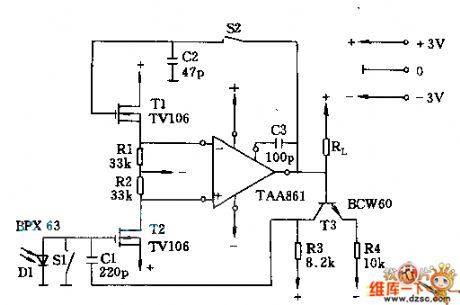
In the situation with minimal light intensity, it is not appropriate to use photosensitive photodiode resistor or general photodiode. It is advised to use dedicated photodiode BPX63 with minimal cut-off current.
In the circuit, the light irradiates on diode D1 continuously. If switches S1 and S2 both close, the photocurrent results in short circuit. At this time, FET T1 and T2 and the resistors R1 and R2 constitute the source emitter follower. When the switch S2 closes, the output of operational amplifier is connected to the input of the anti-body of same phase through the field-effect transistor. If the switches S1 and S2 both open, the strong negative feedback circuit cuts off. But the operating point of field-effect transistor T2 changes.
(View)
View full Circuit Diagram | Comments | Reading(1004)
Operational Amplifier Of Double Power Supply And Single Power Supply Circuit
Published:2011/5/22 2:53:00 Author:Robert | Keyword: Operational Amplifier, Double Power Supply, Single Power Supply


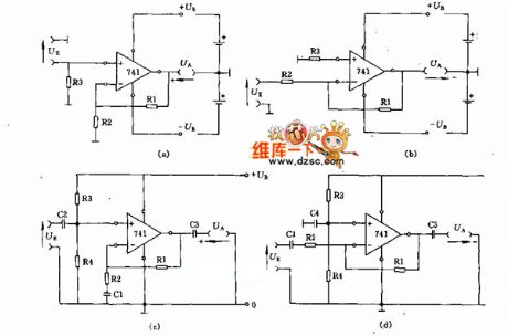
For the circuit in picture (a), it uses double power supply, in-phase input, its amplification factor is:V=+Ua/Ue=(R1+R2)/R2, 1MΩ>R3>10kΩ, R2>1kΩ, V<200.For the circuit in picture (b), it uses double power supply, out-phase input, so:V=Ua/Ue=R1/R2, 1MΩ>R3>10kΩ, R2>1kΩ, V>200.For the circuit in picture (c), it uses single power supply, in-phase input, so:V=+Ua/Ue=(R1+R2)/R2, 1MΩ>R3 and R3>10kΩ, R2>1kΩ, V<200, 1/wC1<0.5R2.For the circuit in picture (d), it uses single power supply, out-phase input, so:V=-Ua/Ue=R1/R2, 1MΩ>R3 and R3>10kΩ, R2>1kΩ, V<200, 1/wC1<0.5R2.
(View)
View full Circuit Diagram | Comments | Reading(826)
Voltage Amplifier Circuit Made up of LF356 and Others
Published:2011/5/20 19:55:00 Author:leo | Keyword: Voltage Amplifier Circuit Made up of LF356 and Others, LF356
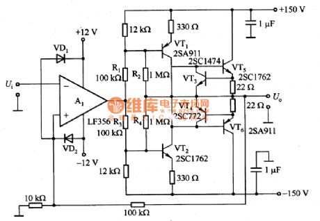
What the picture 1 shows is a voltage amplifier circuit which is made up of LF356 and others. The voltage gain of this circuit is decided by the ratio of R1 and R2( R3 and R4).It can be calculated through the parameters that are shown in the picture that voltage gain is about 20 dB. R1 and R2 can make up of a degenerative circuit which is also be called small local hysteresis loss circuit that can prevent the circuit from close or uncommon oscillation. VD1 and VD2 are protection circuits of input port. (View)
View full Circuit Diagram | Comments | Reading(3730)
| Pages:216/250 At 20201202203204205206207208209210211212213214215216217218219220Under 20 |
Circuit Categories
power supply circuit
Amplifier Circuit
Basic Circuit
LED and Light Circuit
Sensor Circuit
Signal Processing
Electrical Equipment Circuit
Control Circuit
Remote Control Circuit
A/D-D/A Converter Circuit
Audio Circuit
Measuring and Test Circuit
Communication Circuit
Computer-Related Circuit
555 Circuit
Automotive Circuit
Repairing Circuit