
Switch Control
Index 8
TOUCH_ON_OFF_ELECTRONIC_SWITCH
Published:2009/7/8 3:45:00 Author:May

Transistors Q1 and Q2 control latch Q3 and Q4 to switch on the lamp. A high resistance from touching the electrode biases Q1 or Q2 on, setting or resetting the latch. (View)
View full Circuit Diagram | Comments | Reading(893)
TWO_TERMINAL_TOUCH_SWITCH
Published:2009/7/8 3:43:00 Author:May
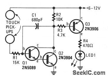
This circuit requires the bridging of two circuits to activate the electronic switch. That circuit does not require a 60-Hz field to operate and can be battery or ac powefed. The two-pickup terminals can be made from most any clean metal; they should be about the size of a penny. The input circuitry of the two-terminal touch switch is a high-gain Darlington amplifier that multiplies the small bridging current to a value of sufficient magnitude to turn on Q3, supplying power to LED1. If a quick on and off switching time is desired, the value of C1 should be very small; if a long on-time period is required, the value of C1 can be increased. (View)
View full Circuit Diagram | Comments | Reading(797)
DIGITAL_TOUCH_ON_OFF_SWITCH
Published:2009/7/8 3:41:00 Author:May
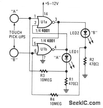
Only one LED can be on when the circuit is at rest. Which LED is illuminated is determined by the touch pick-up that last had human contact. Pickup terminal A controls the on condition of LED1, and terminal B controls the on condition of LED2. A 4001 quad two-input NOR gate is connected in an anti-bounce latching circuit that is activated by touching a pickup. (View)
View full Circuit Diagram | Comments | Reading(1040)
THERMOCOUPLE_WITH_ZERO_VOLTAGE_SWITCH
Published:2009/7/8 1:55:00 Author:May
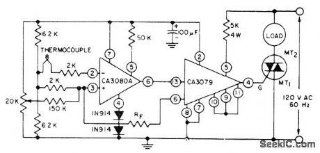
Differential input connection of RCA CA3080A operational transconductance amplifier is used with thernlocouple to drive CA3079 zero-voltage switch serving as trigger for triac handling AC load. Choose triac to match load being controlled. Supply voltage for opamps isnot criticaL.- Linear Integrated Circuits and MOS/FET's. RCA Solid State Division, Somerville, NJ, 1977, p 165-170.
(View)
View full Circuit Diagram | Comments | Reading(1429)
LOW_DISSIPATION_SWITCH
Published:2009/7/8 1:53:00 Author:May
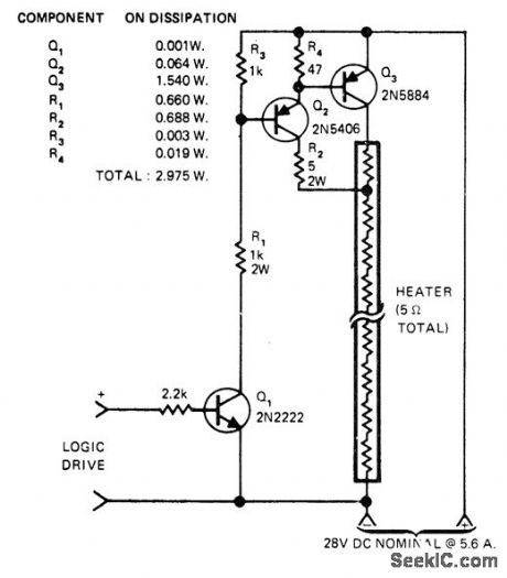
Logic-controlled power switch for 150-W instrument heater uses tap on heating element to force switch Q3, and driver Q2, into saturation and keep dissipation low. When input goes positive, Q1 turns on and drives Q2 and Q3 on. Collector current of Q2, and base drive of Q3 are determined by R2,. Voltage drop across R2 is proportional to supply voltage so drive for Q3 is at optimum level over wide voltage range,-M. Strange, Increase Electronic Power Switch Efficiency, EDN Magazine, Aug.20, 1975, p 78.
(View)
View full Circuit Diagram | Comments | Reading(787)
LINE_ACTIVATED_SOLID_STATE_SWITCH
Published:2009/7/7 22:27:00 Author:May
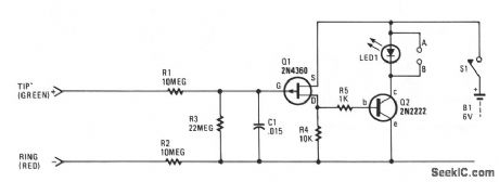
Each and every time a phone on the same line or calling number is taken off-hook, the circuit will be activated to control an extemal electronic circuit. If several extension telephones are used.on one phone line, the circuit can be useful as a busy indicator. LED1 contains a special flashing red LED that makes an excellent indicator for a busy circuit condition.The solid-state switch can be used for several other phone-activated applications, such as automatically tuming on a cassette recorder, starting a phone-use timer or counter, etc. A small relay can be connected at points A and B, in place of LED1, to control extemal circuits. A 117-Vac-to-6-Vdc plug-in power supply can be substituted for the battery to keep the operating cost at a minimum.The 48-Vdc, on-hook, phone-line voltage keeps Q1 in the cut-off condition, allowing no current to flow through resistor R4, hence Q2 remains off. Resistors R1 and R2 keep the solid-state switch circuit from causing any problems with the telephone's central-office equipment. When a phone is taken off-hook, the line voltage (tip to ring) drops to 10 V or less, which forces Q1 to turn on; this, in turn, causes Q2 to trigger LED1, or a relay which might be used in lieu of LED1. (View)
View full Circuit Diagram | Comments | Reading(1261)
MODEL_TRAIN_SWITCHING
Published:2009/7/7 21:58:00 Author:May
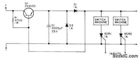
individual SCRs are triggered by logic-level signals independently to initiate discharge of large capacitor C1 through solenoid of model railroad tracks witch.-D. W. zimmerli,Two Hobbies:Model Railroading and Computing,Kilobaud Aug1978,p 62-68. (View)
View full Circuit Diagram | Comments | Reading(1000)
MULTIPLEXING_BCD_SWITCHES
Published:2009/7/7 21:40:00 Author:May
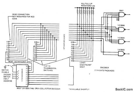
Multiplexing technique reduces number of interconnections between thumbwheel switches and counters, displays, or industrial control equipment being programmed remotely Ten decades of BCD switches require only 10 interconnections, as compared to 50 without multiplexing, All 10outputs of low-cost single-pole decade switches are paralleled. with wiper arm connections being brought out separately Parallel outputs are fed into simple encoder using four NAND gates to generate4-bit BCD output code. Wiper of each switch is addressed from active low open-collector decoder. In operation,3-bit input address determines which decade switch is addressed, and switch position then determines which encoder NAND gates are activated.-E. Breeze, Putting the, ”Thumb″ on Thumbwheel Switch Multiplexing, EDN Magazine, Aug,1,1972, p56. (View)
View full Circuit Diagram | Comments | Reading(1549)
PHOTOELECTRIC_AC_POWER_SWITCH
Published:2009/7/7 21:32:00 Author:May
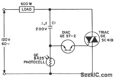
For a dark photocell, high resistance, the voltage across the diac rises rapidly with the line voltage due to the current through C1, triggering the diac early in the cycle.When the photocell resistance is less than about 2000 Ω,the drop across it is limited to less than the diac triggering voltage,and the load power is shut off. (View)
View full Circuit Diagram | Comments | Reading(1777)
SOLAR_TRIGGERED_SWITCH
Published:2009/7/7 21:28:00 Author:May

View full Circuit Diagram | Comments | Reading(711)
LIGHT-CONTROLLED_LAMP_SWITCH
Published:2009/7/7 21:16:00 Author:May
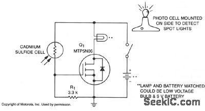
A school drama needed lamps that automatically turned on and off when spot lights did the same.Lamp switching had to be wireless, durable, dependable, simple and inexpensive. With stage and spot lights off, very little light falls on the CdS photocell, so its internal resistance is several megohms and R1 keeps the gate of Q1 at nearly zero volts, which keeps it off. When a spot or stage light hits the photocell, its resistance drops to several hundred ohms, raising Q1's gate voltage, which turns it on and applies power to the lamp. (View)
View full Circuit Diagram | Comments | Reading(993)
SOUND_ACTIVATED_TAPE_SWITCH
Published:2009/7/7 20:38:00 Author:May
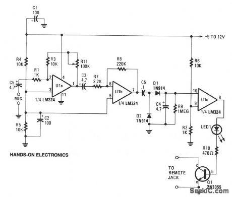
This circuit can cause a cassette recorder to automatically turn on and record when a sound or noise is present. Another use, is when the sound-activated switch is used to turn on a cassette player so that it operates as a burglar-alarm detector and sounder. Op amps U1a and U1b are connected in tandem to amplify the sounds picked up by the detector's mike. The amplified audio voltage, output at pin 7 of U1b, is fed to a voltage-doubler circuit, consisting of D1 and D2. The elevated voltage from the doubler circuit is input to the positive input of op amp U1c, which is operating as a simple comparator circuit. The other input of Ulc is connected to a voltage divider that sets the switching point for the dc signal voltage, to turn on when the signal level is greater than about 1.5 V. As the comparator switches on, its output at pin 8 becomes positive and supplies a forward bias to turn on D3 and Q1, which in turn, starts the recorder. The rc combination of C4/R9 sets the cassette's run time after the input sound has ceased, preventing the recorder from chopping-up or turning-off between closely spaced sounds or words picked up by the mike. The delay time is roughly 6 to 8 seconds. R11 sets the circuit's gain. Connect a low-impedance cassette mike to the amplifier's input, and connect the output of Q1 to the cassette's remote input or to the internal input and set the recorder to the record position. Talk and adjust the amplifier's gain with R11 for the desired sensitivity. (View)
View full Circuit Diagram | Comments | Reading(2671)
SOUND_ACTIVATED_SWITCH
Published:2009/7/7 20:33:00 Author:May
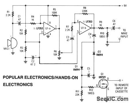
A sensitive electret microphone picks up the sound and feeds the signal to a two-stage amplifter circuit, consisting of U1a and U1b. The amplified output of U1b is fed to a voltage-doubler circuit (comprised of D1, D2, C4, and C5). The output of the doubler is input to the gate of Q1. When the dc voltage reaches the gate's threshold level, Q1 switches on, starting the recorder. Resistor R6 sets the circuit's sensitivity and should be experimented with to obtain the optimum adjustment. (View)
View full Circuit Diagram | Comments | Reading(0)
ANALOG_SWITCH
Published:2009/7/7 20:07:00 Author:May
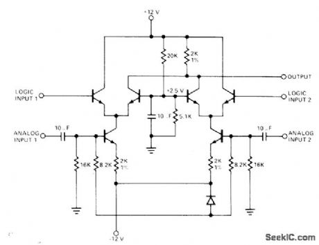
Circuit using Signetics 511 transistor array provides digital selection of either of two analog signals. When logic input at left is zero, signal at analog input 1 goes to output and other analog input signal is rejected. Similarly, when logic 0 is applied to logic input 2, analog input 2 goes to output. Eight-channel analog multiplex switch can be formed by combining four 511 analog switches with Signetics 8250 binary-to-octal decoder. Analog signals up to 200 kHz are switched without amplitude degradation.- Signetics Analog Data Manual, Signetics, Sunnyvale, CA, 1977, p 753-754. (View)
View full Circuit Diagram | Comments | Reading(0)
HALL_EFFECT_SWITCHES
Published:2009/7/7 7:31:00 Author:May
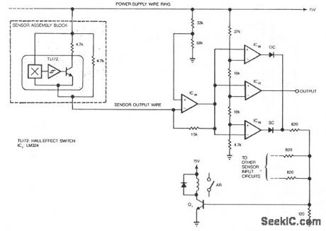
Hall-effect switches have several advantages over mechanical and optically coupled switches. They're insensitive to environmental light and dirt, they don't bind, and they don't sustain mechanical wear. Their major drawback is that they require three wires per device. The circuit shown, however, reduces this wire count to N + 1 wires for N devices.Amplifier IC1A is configured as a current-to-voltage converter. It senses the sensor assembly's out-put current. When the Hall-effect switch is actuated, the sensor's output current increases to twice its quiescent value. Amplifier IC1B, configured as a comparator, detects this increase. The comparator's out-put decreases when the Hall-effect switch turns on.The circuit also contains a fault-detection function. If any sensor output wire is open, its correspond-ing LED will turn on. If the power-supply line opens, several LEDs will turn on. A short circuit will also turn an LED on. Every time an LED turns on, Q1 turns on and the alarm relay is actuated. (View)
View full Circuit Diagram | Comments | Reading(3708)
TOUCH_SWITCH
Published:2009/7/7 5:38:00 Author:May
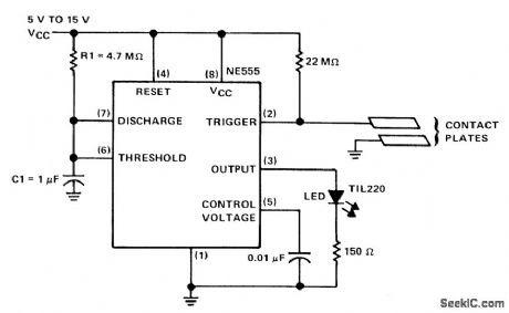
The circuit is basically a NE555 monostable, the only major difference being its method of triggering. The trigger input is biased to a high value by the 22 M ohm resistor. When the contact plates are touched, the skin resistance of the operator will lower the overall impedance from pin 2 to ground. This action will reduce the voltage at the trigger input to below the 1/3 VCC trigger threshold and the timer will start. The output pulse width will be T = 1.1 R1C1, in this circuit about 5 seconds. A relay connected from pin 3 to ground instead of the LED and resistor could be used to perform a switching function. (View)
View full Circuit Diagram | Comments | Reading(0)
TOUCH_ON_OFF_SWITCH
Published:2009/7/7 5:36:00 Author:May
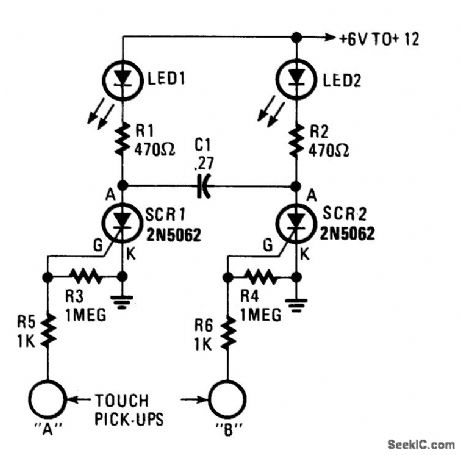
If a Touch On/Off Switch is desired, this circuit fills the bill. Two sensitive gate SCRs are interconnected, so that when one of the devices is turned on, the other (if on) is forced off. That toggling effect gives an on/off circuit condition for each of the LEDs in the SCR-anode circuits. To turn LED1 on and LED2 off, simply touch the A terminal, and to turn LED1 off and LED2 on, the B pick-up must be touched. It is possible to simultaneously touch both terminals, causing both SCRs to turn on together. To reset the circuit to the normal one-on/one-off condition, momentarily interrupt the circuit's dc power source. Additional circuitry can be connected to the anode circuit of either or both SCRs to be controlled by the on/off function of the touch switch. (View)
View full Circuit Diagram | Comments | Reading(1760)
MODEL_RAILROAD_SWITCHING_
Published:2009/7/7 5:05:00 Author:May
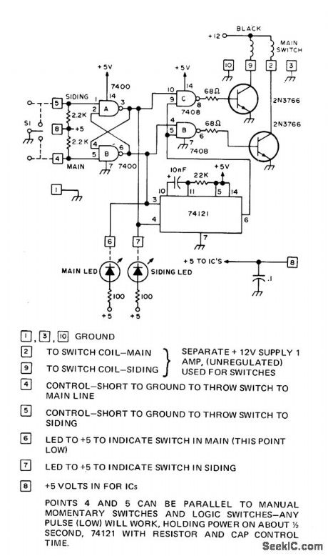
Control circuitis used to drive solenoid-operated track Switches oftγpical HO train layout Inputcan be ρair of comρlementary TTL signals from 8008 orother computer or can be from manual switch s1. 74121 mono MVBR controls time that witch is energized in given direction. Outputcult transistors are rated at 20 W,enough for driving solenoids taking 1 A at 12 V Use protective diodes across coils of solenoids,-H,De Monstoy,Model Railroad Switch Control Circuit,BYTE,Oct .1975,p 87. (View)
View full Circuit Diagram | Comments | Reading(959)
TRIAC_STARTING_SWITCH_FOR_1_2_hp_MOTOR
Published:2009/7/7 3:04:00 Author:May
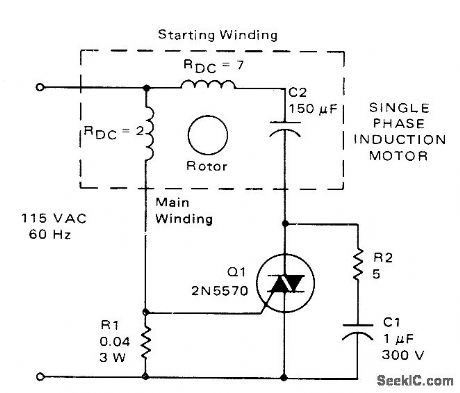
Triac replaces centrifugal switch normally used to control current through starting winding of single-phase induction motor. Value of R1 is chosen so triac turns on only when starting cur-rent exceeds 12A. When motor approaches nor-mal speed, running current drops to 8 A and triac blocks current through starting winding.- Circuit Applications for the Triac, Motorola, Phoenix, AZ, 1971,AN-466, p 8. (View)
View full Circuit Diagram | Comments | Reading(5703)
AC_STATIC_SPDT_SWITCH
Published:2009/7/6 20:11:00 Author:May
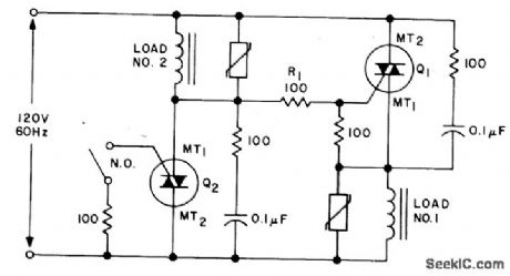
An SPDT solid state relay is shown. When voltage is applied Q1 will tum on, activating load #1, because the full line voltage appears across Q2, supplying gate current through R1. When S1 is closed, Q2 turns on removing the gate drive from Q1 and activating load #2. (View)
View full Circuit Diagram | Comments | Reading(964)
| Pages:8/15 123456789101112131415 |
Circuit Categories
power supply circuit
Amplifier Circuit
Basic Circuit
LED and Light Circuit
Sensor Circuit
Signal Processing
Electrical Equipment Circuit
Control Circuit
Remote Control Circuit
A/D-D/A Converter Circuit
Audio Circuit
Measuring and Test Circuit
Communication Circuit
Computer-Related Circuit
555 Circuit
Automotive Circuit
Repairing Circuit