
Switch Control
Index 13
SWITCH_CLOSURE_CIRCUIT
Published:2009/6/18 3:58:00 Author:May
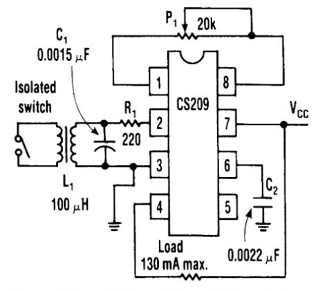
A standard proximity detector circuit for the Cherry Semiconductor CS209 IC can detect an iso-lated switch closure by adding a few tums of wire around the circuit's inductor (Radio Shack 273-102). Moreover, the technique doesn't require any isolated power (see the figure). With the switch open, the potentiometer P1 is adjusted until the output switches off. When the switch is closed, the Q of the circuit changes and the output turns on. Capacitor C1 should be silvered mica, and poten-tiometer P1 should be a multiturn type such as the Boums 3006P-1-203. A 9-V supply can be used for Vcc. (View)
View full Circuit Diagram | Comments | Reading(1120)
DUAL_CONTROL_SWITCH_USES_ac_SIGNALS
Published:2009/6/17 3:37:00 Author:May
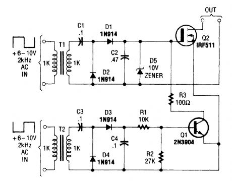
The Dual-Control Switch uses two 6-10-Vac sources to trigger the circuit on and off; one source for each function. (View)
View full Circuit Diagram | Comments | Reading(771)
LOAD_SENSING_SOLID_STATE_SWITCH
Published:2009/6/17 3:17:00 Author:May
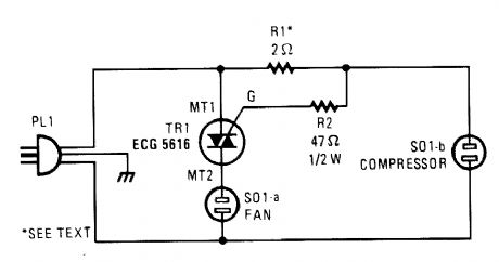
When this triac circuit senses current flow through SOl-a, it activates the device plugged into SOl-b. The values of the resistors must be chosen for the specific devices to be plugged in. (View)
View full Circuit Diagram | Comments | Reading(936)
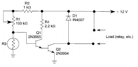
SIMPLE_NONLATCHING_PHOTOCELL_SWITCH
Published:2009/6/17 2:41:00 Author:May
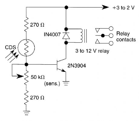
A CDS photocell is used to drive the relay.The circuit operates from a +12 V supply. (View)
View full Circuit Diagram | Comments | Reading(2289)
DARK_ACTIVATED_SWITCH
Published:2009/6/17 2:34:00 Author:May
In this circuit, lowering of the light level on the CDS cell turns on Q1 and Q2 which switches on the load which could be a relay, light, etc. (View)
View full Circuit Diagram | Comments | Reading(133)
COMBINED_LIGHT__DARK_ACTIVATED_SWITCH
Published:2009/6/17 2:30:00 Author:May
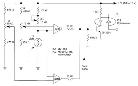
Two op arnps used in a bridge circuit configuration detect high and low light levels. Potentiometer R2 sets the dark level and R1 controls the light level. R3 is set so that about 1/2 the supply voltage appears across R4 at the desired light level. R1 and R2 set the trip point of the optoisolator IC2 at darker or lighter ambient levels, as required. (View)
View full Circuit Diagram | Comments | Reading(1102)
IR_CONTROLLED_REMOTE_A_B_SWITCH
Published:2009/6/16 22:11:00 Author:May
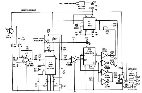
Useful for A/B control, the IR receiver shown controls a relay from an infrared beam that has a pulsed tone-modulated signal. Q1 is the photo receptor feeding op amp IC1, tone decoder IC2, and flip-flop IC3. IC5 turns off the indicator LEDs after about 15 seconds. (View)
View full Circuit Diagram | Comments | Reading(1178)
LAMP_SWITCHING_CIRCUIT
Published:2009/6/16 2:49:00 Author:May
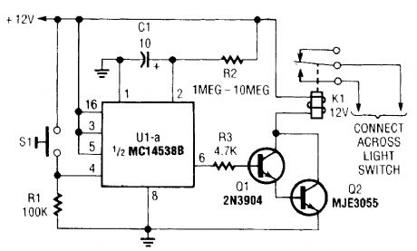
A normally open pushbutton switch (51) delivers a positive input pulse to pin 4 of U1, triggering the IC into action. The output of U1 at pin 6 supplies base-drive current to a Darlington pair comprised of Q1 and Q2, activating K1. A 10-μF capacitor and any resistor value of from 1 to 10 MΩ can be used as the timing components.To use the circuit on an auto's headlights, connect the relay's normally open contacts across the car's headlight switch and press S1 to extend the on time. In connecting the circuit to control an acoperated lamp, turn off the ac power and connect the relay contacts in parallel with the lamp's power switch contacts. (View)
View full Circuit Diagram | Comments | Reading(894)
ELECTRONIC_DOORBEL
Published:2009/6/16 1:56:00 Author:May
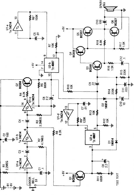
When the doorbell switch is pressed,the two monostable stages are activated in sequence,appling bias to a pair of voltagecontrolled resistor stages.These then modulate the outputs fro, a pair of tone generators.The resulting signals are fed to an audio amplifier,then to the speaker. (View)
View full Circuit Diagram | Comments | Reading(801)
BCD_ROTARY_SWITCH
Published:2009/6/15 23:11:00 Author:May
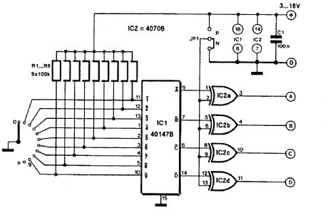
This circuit allows a simple rotary switch to emulate a BCD switch. The circuit draws about 200 mA. A 10-position rotary switch is used. (View)
View full Circuit Diagram | Comments | Reading(5002)
DIGITAL_AUDIO_SELECTOR
Published:2009/6/15 23:05:00 Author:May
This circuit uses switched emitter followers, rather than the usual analog switch CMOS chips. This yields better reduction of crosstalk between channels. This circuit can handle up to 4 Vrms with less than -80-dB crosstalk. (View)
View full Circuit Diagram | Comments | Reading(1510)
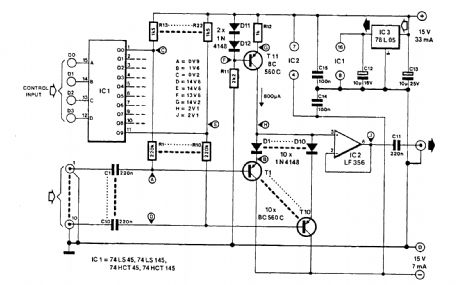
DIGITAL_ENTRY_LOCk
Published:2009/6/15 23:00:00 Author:May

A block pinout diagram of the LS7220 keyless-lock IC is shown. The keypad must provide each key with a contact to a common connection. In this case, the common connection goes to the posi-tive supply rail so that when a key is pressed, a positive voltage is passed through to the wire associ-ated with that key. Each of the 12 keys are brought out to separate wires, and each wire is connected to a different pin of a 24-pin socket (SO1).To activate (unlock) the circuit, a preprogrammed four-digit access code must be entered in the proper sequence. The four-digit access code must be entered in the proper sequence. The four-digit access is programmed into the' circuit by connecting jumpers between terrrtinals of a 24-pin plug-in header.When the correct access code is entered (in the proper sequence), positive voltages appear at pins 3, 4, 5, and 6 of U1. That causes U1 to output a positive voltage at pin 13, which is fed through resistor R2 to the base of Q1, causing it to conduct. With Q1 conducting, its collector is pulled to ground potential, energizing relay K1. The normally open relay contacts close, switching on any ex-ternal device.Capacitor C2 controls the total time that the output of U1 at pin 13 is positive after the release of the first key. With avalue of 3.3 pF for C2, active time after release of the first key is about two sec-onds, assuming a 6-V supply or four seconds with a 12-V supply. Therefore, if you push the subse-quent keys too slowly, the relay might not close at all! To increase the time allotted for code entry, you will have to increase the capacitance of C2. (View)
View full Circuit Diagram | Comments | Reading(2)
AUTOMATIC_TR_SWITCH
Published:2009/6/15 21:11:00 Author:May
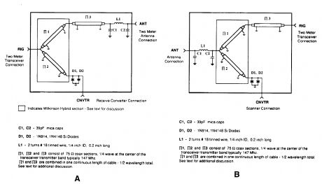
A pair of diodes and a quarter-wave transmission line are used as an automatic TR switch. D1 and D2 conduct during transmit periods, short-circuiting the scanner input. In th 1/4-wave line appears as an open circuit. In receive, the circuit acts as a Wilkinson power divider. (View)
View full Circuit Diagram | Comments | Reading(1036)
THERMOSTAT_SWITCH_FOR_AUTOMOTIVE_ELECTRIC_FANS
Published:2009/6/14 22:25:00 Author:May
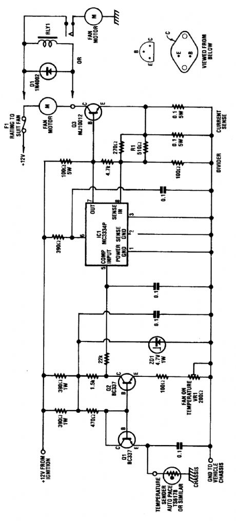
The circuit is based on a commercial temperature sensor(TS6178) and an MC3334P ignition chip. When the radiator temperature increaser,the sensor pulls the base of Q2 low via Q1, which is wired as a diode.Q2's collector thus goes high and riggers IC1,which switches its pin 7 output high and turns on the fan motor via Q3. (View)
View full Circuit Diagram | Comments | Reading(1529)
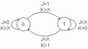
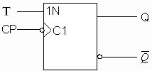
Trigger Circuit of Devices
Published:2011/7/16 0:41:00 Author:Felicity | Keyword: Trigger
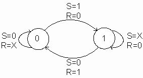
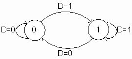
We have three ways to describe the logical function of trigger. First is characteristic equation. Second is characteristic table and the third one is state transition diagram. (showed in picture 1,2,3,4)
Picture 1 shows the state transition diagram of RS Trigger.
Picture2 shows the state transition diagram ofJK Trigger.
Picture3 shows the state transition diagram and logical symbol ofJK Trigger.
Picture4 shows the state transition diagram ofD Trigger.
Characteristics table is actually a special kind of truth table and it has a very specific description of trigger.The input variables (independent variables)of truth table are not only data entry but also initial states of flip-flop. And the output variable (dependent variable) is the next state flip-flop. Characteristic equation is out from the feature table summarizes so it's more concise. State transition diagramwhich describes the methodsis very intuitive. (View)
View full Circuit Diagram | Comments | Reading(805)
Multi-Channel Corded Remote-Control Switch Circuit
Published:2011/7/18 9:34:00 Author:Robert | Keyword: Multi-Channel, Corded, Remote-Control, Switch
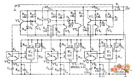
The picture shows the multi-channel corded remote-control switch circuit. (View)
View full Circuit Diagram | Comments | Reading(811)
Electronic Switch And Driving Circuit
Published:2011/7/17 8:14:00 Author:Robert | Keyword: Electronic, Switch, Driving
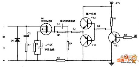
The picture shows the electronic switch and driving circuit. (View)
View full Circuit Diagram | Comments | Reading(649)
Switching circuit diagram with photocoupler
Published:2011/5/13 4:16:00 Author:Ecco | Keyword: Switching circuit, photocoupler
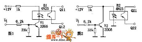
According to the figure 1, when the input signal ui is in low level, the transistor V1 is placed in a closed state, the current of LED in photocoupler B1 is nearly 0, the resistance between Q11 and Q12 is so high to result in the switch be off ; When the ui is in high level, the LED of Bi is lit, the resistance between Q11 and Q12 becomes low,the switchis switch on . As Ui is in low level, switch is impassable, the circuitry is in high level conducting state. In the same argument, in the figure 2, because of having no semaphore(Ui for low level), switch turns on, the circuitry is in low level conducting state.
(View)
View full Circuit Diagram | Comments | Reading(695)
Simple and practical touch delay switch circuit
Published:2011/6/13 21:38:00 Author:Fiona | Keyword: Simple and practical, touch delay switch
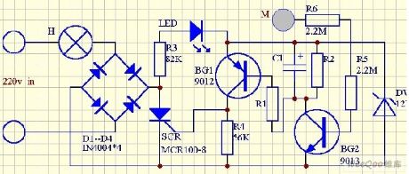
Delay switch circuit is shown in Figure D1 - D1, SCR component switch is composed of main circuit, BG1, BG2 switch and other components switches are composed of the control circuit. Switching delay time is mainly determined by the value of the resistance R1, R2 and capacitor C1. Provide a group of experimental data below for reference.If it want to further increase delay time, it can increase the capacity of C1. In addition to these major factors, BG1 magnification and the trigger sensitivity of the SCRare also affected to delay time. (View)
View full Circuit Diagram | Comments | Reading(1013)
Proximity Switch Circuit Composed Of Integrated Magnetic Sensor HMC1001
Published:2011/7/7 6:52:00 Author:Robert | Keyword: Proximity, Switch, Integrated, Magnetic Sensor
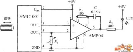
The picture shows the proximity switch circuit composed of the HMC1001 and operational amplifier (AMP04) and light emitting diode (LED). The operational amplifier is used as a comparator here. If taking a magnet with length about 6mm~12mm to close to the HMC1001, when it moves to a certain position, the MR electric bridge's output voltage would be 30mV to flip the comparator and then it outputs low voltage level to make LED light. If remove the magnet the comparator would output high voltage level to stop LED lighting. Obviously, the circuit is equivalent to the proximity switch with indicating light. It can be used for detecting displacement, rotating speed and other non-electricity parameter. By adjusting R1's resistance value it can set the switch's threshold voltage. (View)
View full Circuit Diagram | Comments | Reading(2924)
| Pages:13/15 123456789101112131415 |
Circuit Categories
power supply circuit
Amplifier Circuit
Basic Circuit
LED and Light Circuit
Sensor Circuit
Signal Processing
Electrical Equipment Circuit
Control Circuit
Remote Control Circuit
A/D-D/A Converter Circuit
Audio Circuit
Measuring and Test Circuit
Communication Circuit
Computer-Related Circuit
555 Circuit
Automotive Circuit
Repairing Circuit