
Circuit Diagram
Index 1321
SRABLE_HIGH_IMPEDANCE_BUFFER
Published:2009/6/24 22:50:00 Author:May
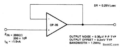
View full Circuit Diagram | Comments | Reading(546)
DARKROOM_TIMER
Published:2009/6/24 23:13:00 Author:Jessie
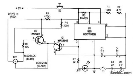
The electronic darkroom timer is built around a 555 oscillator/timer, a pair of general-purpose transistors, a buzzer, and an LED. The 555 (U1) is configured as an astable multivibrator (free-rututing oscillator). The frequency of the oscillator is determined by the values R1 through R3 and C1 through C4.
Switch S1 is used to divide the capacitor network to vary the time interval between beeps; when S1 is closed, the circuit beeps at intervals of 30 seconds. With S1 closed, it beeps at 15-second intervals.
When power is applied to the circuit (by closing switch S2), the output of U1 at pin 3 is initially high. That high is applied to the base of transistor Q1 (an MPS2907 general-purpose pnp device), keeping it turned off. That high is also applied to the anode of LED1 (which is used as a power on indicator) through resistor R7, turning it on.
Timing capacitors C1 through C5 begin to charge through timing resistors R1 through R3. dc voltage is applied to BZ1's driver input through R5 and to its feedback terminal (through R4), which is also connected to Q2's base terminal. The V+ voltage that applied to Q2's base causes it to turn on, tying BZ1's common terminal high.
When the timing capacitors are sufficiently charged, a trigger pulse is applied to pin 2 (the trigger input) of U2, causing U1's output to momentarily go low. This causes LED1 to go out and tran-sistor Q1 to turn on. That, in turn, grounds the common lead of buzzer BZ1, causing BZ1 to sound. Afterward, the output of U1 returns to the high state, turning off Q1, and turning on LED1, until another time interval has elapsed and the process is repeated.
The circuit is powered by a 9-Vac adapter, which plugs into a standard 117-V household outlet. Because the circuit draws only about 10 to 15 mA, a 9-V alkaline transistor-radio-battery can also be used to power the circuit. (View)
View full Circuit Diagram | Comments | Reading(3367)
CRYSTAL_CONTROLLED_BUTLER_OSCILLATOR
Published:2009/6/24 23:13:00 Author:Jessie
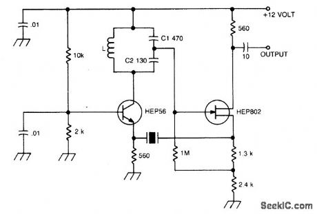
Circuit NotcsA typical Butler oscillator (20-100 MHz) uses an FET in the second stage; the circuit is not reliable with two bipolars. Sometimes two FETs are used. Frequency is determined by LC values. (View)
View full Circuit Diagram | Comments | Reading(1888)
CMOS_BIPOLAR_VOLTAGE_FOLLOWER
Published:2009/6/24 23:12:00 Author:Jessie
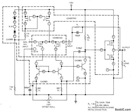
Combination of two 4007 CMOS gate packages andone CA3083 transistor package provides gain of about 75 dB as voltage-follower amplifier and bandwidth of 50 kHz. Slew rate is about 30V/μs, and settling time is 2 ps. Requires only single +15 V supply. Can be driven to within 1 mV of ground. Interfaces well with singlsupply D/A converters.-B. Furlow, CMOS Gates in Linear Applications: The Results Are Surpris-ingly Good, EDN Magazine, March 5, 1973, p 42-48. (View)
View full Circuit Diagram | Comments | Reading(1087)
LATCHING,DOUBLE_BUTTON_TOUCH_SWITCH
Published:2009/6/24 23:11:00 Author:Jessie
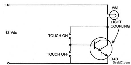
View full Circuit Diagram | Comments | Reading(1197)
Indudes_general
Published:2009/6/24 23:11:00 Author:Jessie
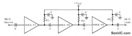
purpose RF amplifiers covering various portions of spectrum from DC to 2.3 GHz at outputs up to 230W, some with voltage-controlled gain, for pulses as well as video and other RF signals. See other chapters in book for RF amplifiers having specific applications.
0.25-400 MHz CASCADE-Three hybrid nlodules in cascade provide gain of 43.5 dB with flatness of ±1 dB over frequency range. Circuit draws 44 mA from 12-VDC supply. Modules 1 and 2 are Motorola MWA110, and module 3 is MWA120. All capacitors are 0.018μF. R1 and R2 are 1K,and R3 is 300 ohms,-“Wideband HybridAmplifiers、”Motorola,Phoenix,AZ, 1978、DS 5712 (View)
View full Circuit Diagram | Comments | Reading(826)
CMOS_TOUCH_SWITCH
Published:2009/6/24 23:10:00 Author:Jessie
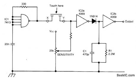
This touch switch does not rely on mains hum for switching. It can be used with battery powered circuits. Schmitt trigger IC1 forms a I 100 kHz oscillator and IC2a which is biased into the linear region, amplifies the output and charges C1 via the diode. IC2b acts as a level detector. When the sensor is touched, the os-cillator signal is severely attenuated which causes C1 to discharge and IC2b to change state. (View)
View full Circuit Diagram | Comments | Reading(2064)
TOUCH_CIRCUIT
Published:2009/6/24 23:10:00 Author:Jessie
View full Circuit Diagram | Comments | Reading(1326)
PTOXIMITY_DETECTOR
Published:2009/6/24 23:09:00 Author:Jessie
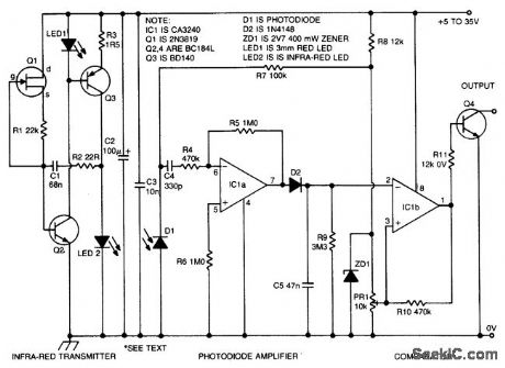
The proximity sensor works on the principle of transmitting a beam of modulated infra-red light from the emitter diode LED2, and receiving reflections from objects passing in front of the beam with a photodiode detector D1. The circuit can be split into three distinct stages; the infra-red transmitter, the photodiode amplofoer, and a variable threshol comparator. (View)
View full Circuit Diagram | Comments | Reading(1806)
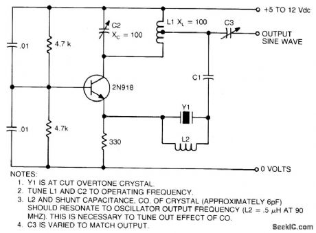
FIFTH_OVERTONE_OSCILLATOR
Published:2009/6/24 23:06:00 Author:Jessie
Circuit NotesThis circuit isolates the crystal from the dc base supply with an rf choke for better starting characteristics. (View)
View full Circuit Diagram | Comments | Reading(1362)
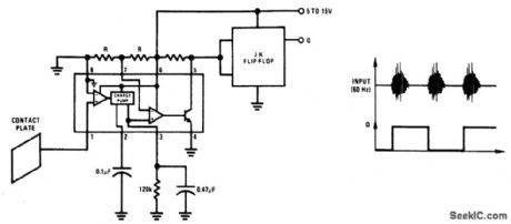
FINGER_TOUCH_OR_CONTACT_SWITCH
Published:2009/6/24 23:05:00 Author:Jessie
View full Circuit Diagram | Comments | Reading(723)
TOUCH_SWOTCH_OR_PROXIMITY_DETECTOR
Published:2009/6/24 23:04:00 Author:Jessie
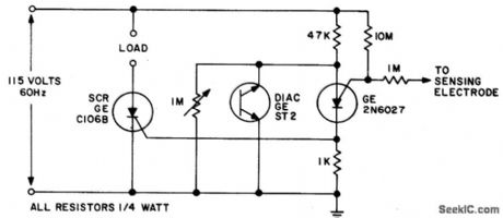
This circuit is actuated by an increase in capacitance between a sensing electrode and the ground side of the line. The sensitivity can be adjusted to switch when a human body is within inches of the insulated plate used as the sensing electrode. Thus, sensitivity is adjusted with the 1 megohm potentiometer which de-termines the anode voltage level prior to clamping. This sensitivity will be proportional to the area of the surface opposing each other. (View)
View full Circuit Diagram | Comments | Reading(1389)
SELF_BIASED_PROXIMITY_SENSOR_WORKS_ON_DETECTED_CHANGING_FIELD
Published:2009/6/24 23:03:00 Author:Jessie
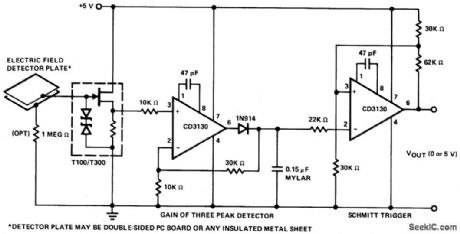
View full Circuit Diagram | Comments | Reading(0)
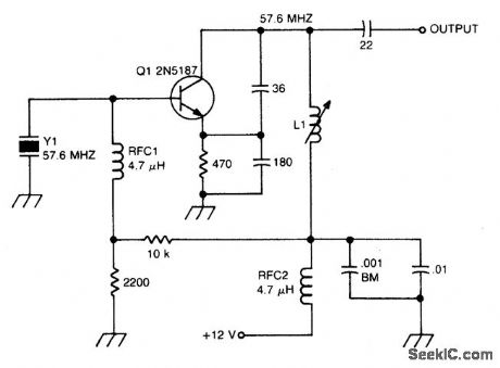
50_MHz_150_MHz_OVERTONE_OSCILLATOR
Published:2009/6/24 23:02:00 Author:Jessie
View full Circuit Diagram | Comments | Reading(1204)
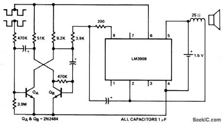
CAPACITANCE_OPERATED_ALARM_TO_FOIL_PURSE_SNATCHERS
Published:2009/6/24 23:01:00 Author:Jessie
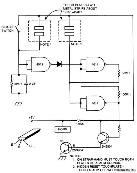
Aslong as touch plates (1) are touched together,the alarm is off. If not held for about 30 seconds,the alarm goes off. The circuit can be disabled with switch or by touching the plates (2),The alarm is battery operated by a bicycle horn. (View)
View full Circuit Diagram | Comments | Reading(1322)
PHOTO_STROBE
Published:2009/6/24 23:00:00 Author:Jessie
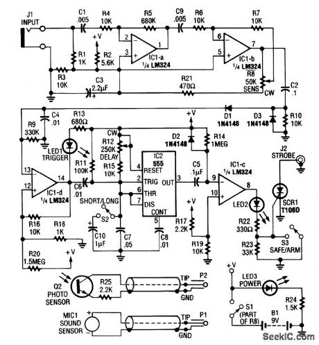
Sound or light sensors connected to J2 produce a voltage that is amplified by IC1-a and IC1-b. A positive trigger voltage that is developed by D1 and D3 and amplified by IC1-d, drives IC2 and IC1 to trigger SCR1. SCR1 is connected to a strobe. This device is handy for photographic purposes to take pictures of events that involve sound, such as impacts, etc. (View)
View full Circuit Diagram | Comments | Reading(1417)
100_×_BUFFER_AMPLIFIER
Published:2009/6/24 22:49:00 Author:May
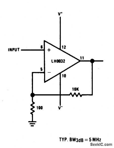
View full Circuit Diagram | Comments | Reading(592)
HIGH_RESOLUTION_ADC_INPUT_BUFFER
Published:2009/6/24 22:47:00 Author:May

View full Circuit Diagram | Comments | Reading(655)
HIGH_SPEED_6_BIT_A_D_BUFFER
Published:2009/6/24 22:47:00 Author:May
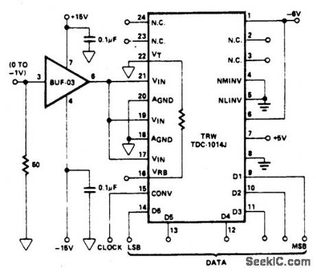
View full Circuit Diagram | Comments | Reading(569)
PHOTO_FLASH_SLAVE_UNIT
Published:2009/6/24 22:46:00 Author:May
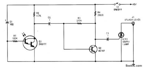
Phototransistor Q1 receives a light pulse from a photoflash unit. The pulse is accoupled to am-plifier Q2. It then triggers SCR1, which triggers a flash unit that is connected to J1. (View)
View full Circuit Diagram | Comments | Reading(1393)
| Pages:1321/2234 At 2013211322132313241325132613271328132913301331133213331334133513361337133813391340Under 20 |
Circuit Categories
power supply circuit
Amplifier Circuit
Basic Circuit
LED and Light Circuit
Sensor Circuit
Signal Processing
Electrical Equipment Circuit
Control Circuit
Remote Control Circuit
A/D-D/A Converter Circuit
Audio Circuit
Measuring and Test Circuit
Communication Circuit
Computer-Related Circuit
555 Circuit
Automotive Circuit
Repairing Circuit