
Circuit Diagram
Index 1320
PHOTO_STROBE
Published:2009/6/24 23:00:00 Author:May
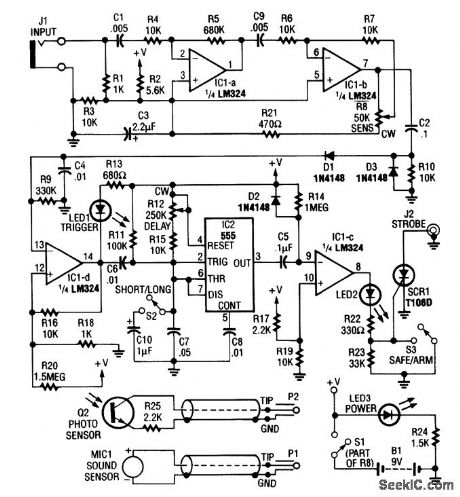
Sound or light sensors connected to J2 produce a voltage that is amplified by IC1-a and IC1-b. A positive trigger voltage that is developed by D1 and D3 and amplified by IC1-d, drives IC2 and IC1 to trigger SCR1. SCR1 is connected to a strobe. This device is handy for photographic purposes to take pictures of events that involve sound, such as impacts, etc. (View)
View full Circuit Diagram | Comments | Reading(0)
TOUCH_TRIGGERED_BISTABLE
Published:2009/6/24 22:59:00 Author:May
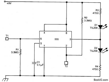
This circuit uses a 555 timer in the bista-ble mode. Touching T2 causes the output to go high; D2 conducts and Dl extinguishes. Touching T1 causes the output to go low; Dl conducts and D2 is cut off. The output from pin 3 can also be used to operate other circuits (e.g., a triac controlled lamp). In this case, the LEDs are useful for finding the touch terminals in the dark. C1 is not absolutely necessary but helps to prevent triggering from spurious pulses. (View)
View full Circuit Diagram | Comments | Reading(841)
MOMENTARY_OPERATION_TOUCH_SWITCH
Published:2009/6/24 22:59:00 Author:May
View full Circuit Diagram | Comments | Reading(857)
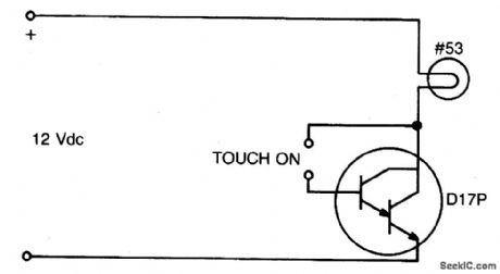
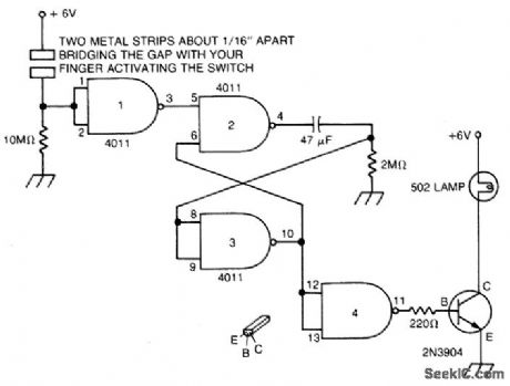
CAPACITANCE_SWITCHED_LIGHT
Published:2009/6/24 22:58:00 Author:May
The battery powered light turns on easily, stays on for just a few seconds, and then turns off again. The circuit is triggered when you place a finger across the gap between two strips of metal, about 1/16th inch apart. Enough current will flow through your finger to trigger the SCR after being amplified by the 2N3906. Once the SCR is fired, current will flow through the bulb until its internal bimetal switch tums it off. 0nce that happens, the SCR will return to its nonconducting state. (View)
View full Circuit Diagram | Comments | Reading(893)
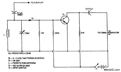
IC_CARRIER_CURRENT_TRANSMITTER
Published:2009/6/24 23:29:00 Author:Jessie

View full Circuit Diagram | Comments | Reading(1513)
SCHMITT_TRIGGER_CSCILLATOR
Published:2009/6/24 22:57:00 Author:May
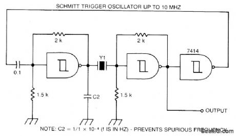
Circuit NotesA Schmitt trigger provides good squaring of the output, sometimes eliminating the need for an extra output stage. (View)
View full Circuit Diagram | Comments | Reading(956)
CARRIER_CURRENT_TRANSMITTER_1
Published:2009/6/24 23:25:00 Author:Jessie
View full Circuit Diagram | Comments | Reading(1461)
CARRIER_CURRENT_TRANSMITTER
Published:2009/6/24 23:24:00 Author:Jessie

View full Circuit Diagram | Comments | Reading(1870)
LOW_CURRENT_TOUCH_SWITCH
Published:2009/6/24 22:57:00 Author:May
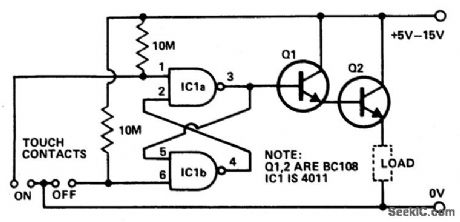


Touching the on contacts with a finger brings pin 3 high, pair and supplying power to the load (transistor radio etc). transistor, and Q2 is chosen for the current required by the turning on the Darlington Q1 must be a high gain load circuit. (View)
View full Circuit Diagram | Comments | Reading(746)
CARRIER_CURRENT_RECEIVER
Published:2009/6/24 23:21:00 Author:Jessie

160 kHz transformer consists of a 18 x 11mm ungapped pot core (Siemens, Ferrocube, etc.), itilizing magnerics incorporated type F material wond woth 80 1/2 turns of No.35 sire for the secondary and 5 1/2 turns for the primary. This gives a turns ratio fo approximately 15 to 1. (View)
View full Circuit Diagram | Comments | Reading(3361)
TOUCH_SENSITIVE_SWITCH
Published:2009/6/24 22:56:00 Author:May
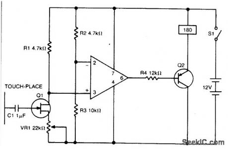
A high impedance input is provided by Q1, a general purpose field effect transistor. 741 op amp is used as a sensitive voltage level switch which in turn operates the current Q2, a medium current PNP bipolar transistor, thereby energizing the relay which can be used to control equipment, alarms, etc. (View)
View full Circuit Diagram | Comments | Reading(2035)
OVERTONE_OSCILLATOR_WITH_CRYSTAL_SWITCHING
Published:2009/6/24 23:18:00 Author:Jessie

Circuit Notes
The large inductive phase shift of L1 is compensated for by C1. Overtone crystals have very narrow bandwidth; therefore, the trimmer has a smaller effect than for fundamental-mode operation. (View)
View full Circuit Diagram | Comments | Reading(1379)
CAPACITANCE_OPERATED_BATTERY_POWERED_LIGHT
Published:2009/6/24 22:55:00 Author:May
Touch the plate and the light will go on and remain on for a time determined by the time constant of the 47 μF capacitor and the 2M resistor. (View)
View full Circuit Diagram | Comments | Reading(817)
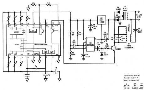
200_kHz_LINE_CARRIER_TRANSMITTER_WITH_ON_OFF_CARRIER_MODULATOR
Published:2009/6/24 23:16:00 Author:Jessie
View full Circuit Diagram | Comments | Reading(2438)
CAPACITANCE_RELAY
Published:2009/6/24 22:54:00 Author:May
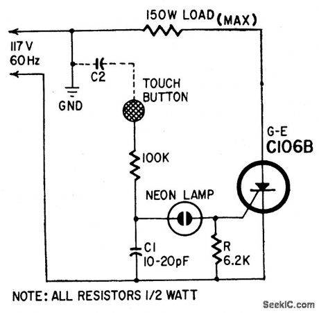
Capacitor C1 and body capacitance (C2) of the operator form the voltage divider from the hot side of the ac line to ground. The voltage across C1 is determined by the ratio of C1 to C2. The higher voltage is developed across the smaller capacitor. When no one is close to the touch button, C2 is smaller than C1. When a hand is brought close to the button, C2 is many times larger than C1 and the major portion of the line voltage appears across C1. This vol-tage fires the neon lamp, C1 and C2 discharge through the SCR gate, causing it to trigger and pass current through the load. The sensitivity of the circuit depends on the area of the touch plate. When the area is large enough, the cir-cuit responds to the proximity of an object rather than to touch. C1 may be made variable so sensitivity can be adjusted. (View)
View full Circuit Diagram | Comments | Reading(1048)
ENLARGING_LIGHT_METER
Published:2009/6/24 22:52:00 Author:May

Meter M1, a +/-50-μA zero-center D'Arsonval meter movement is driven by U1, a TL081 FET op amp, through R3. The gain of UI is set at 11 by R1 and R2, while capacitor C1 is used to restrict the bandwidth of U1 to 1.6 Hz. Power for the circuit is derived from a simple dual-polarity 12-V power supply (consisting of T1, D3, D4, C2, and C3).
A light-dependent resistor (LDR), R16 (which is a semiconductor element whose resistance decreases as it is exposed to increasing illumination), is used as a light-sensing device. One end of R16 is connected to the negative supply rail through R12, and the other end is connected to pin 3 of U1, applying a negative current to U1. A variable (over a 4:1 range) positive current determined by the settings of R14 and S1 (and derived from the positive supply rail) is also fed to pin 3 of U1.
When the two currents (of opposite polarities) are equal, they cancel each other out, so effectively no current is applied to pin 3 of U1. With no current applied to pin 3, the output of U1 is zero and meter M1 registers accordingly, indicating a null. However, when light striking R16 causes its re-sistance to decrease, the current through the device increases, making the negative current greater than the positive current. Under that condition, the negative current causes the output of U1 to swing negative, causing the pointer to swing in the negative direction.
That indicates that the light intensity must be reduced by using a smaller lens opening on the en-larger (smaller f/stop). The opposite occurs if the light is too dim. Lamp 11, a 12-V 60-mA grain of wheat unit, is used to illuminate the meter scale, and R15 is used to limit the meter's illumination to a faint glow that is just bright enough so that the face of M1 can be plainly seen in a photo darkroom. Resistors R3 and R4 should be selected for the meter used. With a dual supply of +/-12 V, U1 produces an output voltage of 10 V peak-to-peak. The resistance of R3 can be found by dividing the peak voltage (i.e., 10/2) by the full-scale meter current (in amps); i.e., R3 = (10/2)/0.0005 = 100,000 Ω. R4, the shunt resistor, should be selected to have a value equal to the meter's internal resistance. (View)
View full Circuit Diagram | Comments | Reading(1593)
PHOTO_STROBE_SLAVE_TRIGGER
Published:2009/6/24 23:14:00 Author:Jessie
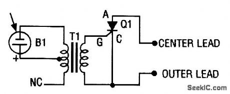
The photo strobe slave trigger circuit uses a solar cell and an SCR to flash any strobe when you trigger your master strobe. The tiny solar cell produces a vet'y small voltage when light falls on its surface. (View)
View full Circuit Diagram | Comments | Reading(1518)
Carrier_System_Transmitter
Published:2009/6/24 23:14:00 Author:Jessie
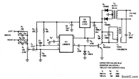
High quality, noise free, wireless FM transmitter/receiver operates over standard power lines. Complete system is suitable for high-quality transmission of speech or music, and will operate from any ac outlet anywhere on a one-acre homesite. Frequency response is 20-20, 000 Hz and THD is under 1/2%. Transmission distance along a power line is at least adequate to include all outlets in and around a suburban home and yard.Two input terminals are provided so that both left and right signals of a stereo set may be combined for mono transmission to a single remote speaker if desired. (View)
View full Circuit Diagram | Comments | Reading(2781)
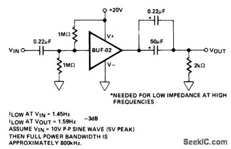
HIGH_SPEED_SINGLE_SUPPLY_AC_BUFFER
Published:2009/6/24 22:52:00 Author:May
View full Circuit Diagram | Comments | Reading(661)
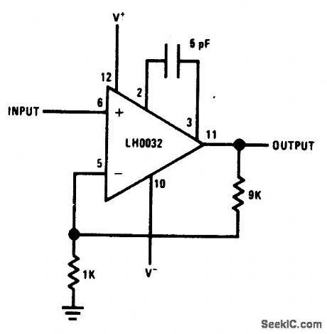
10_×_BUFFER_AMPLIFIER
Published:2009/6/24 22:51:00 Author:May
View full Circuit Diagram | Comments | Reading(608)
| Pages:1320/2234 At 2013011302130313041305130613071308130913101311131213131314131513161317131813191320Under 20 |
Circuit Categories
power supply circuit
Amplifier Circuit
Basic Circuit
LED and Light Circuit
Sensor Circuit
Signal Processing
Electrical Equipment Circuit
Control Circuit
Remote Control Circuit
A/D-D/A Converter Circuit
Audio Circuit
Measuring and Test Circuit
Communication Circuit
Computer-Related Circuit
555 Circuit
Automotive Circuit
Repairing Circuit