
Circuit Diagram
Index 1309
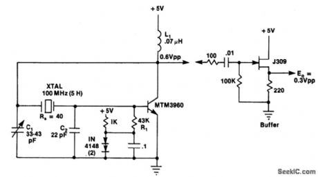
PIERCE_HARMONIC_OSCILLATOR(100_MHz)
Published:2009/6/25 3:10:00 Author:May
Circuit Notes
The output resistance of the transistor's collector, together with the effective value of C1, provides an RC phase lag of 30-500. The crystal normally oscillates slightly above series resonance, where it is both resistive and inductive. Above series resonance, the crys-tal's internal impedance (resistive and induc-tive) together with C2 provides an RLC phase lag of 130-1500. The transistor inverts the sig-nal, providing a total of 3600 of phase shift around the loop. Inductor L1 is selected to resonate with C1 at a frequency between the crystal's desired harmonic and its next lower odd harmonic. Inductor L1 offsets part of the negative reactance of C1 at the oscillation fre-quency. (View)
View full Circuit Diagram | Comments | Reading(1433)
PROGRAMMABLE_GATE
Published:2009/6/25 3:10:00 Author:May
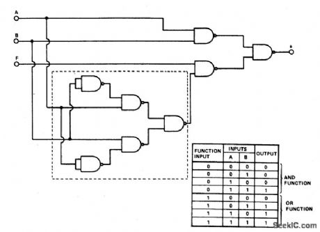
This gate converts an AND gate or an OR gate by applying a logic '1' on the function input. The logic design uses 8 two-input NAND gates. The number of gates may be reduced by replacing the 5 NAND gates enclosed by the dotted line with a two-input exclusive-OR, such as the TTL 7486. (View)
View full Circuit Diagram | Comments | Reading(1022)
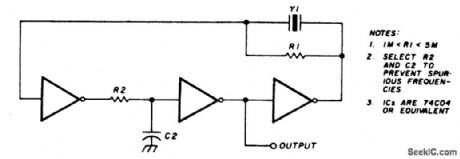
CMOS_OSCILLATOR_1_MHz_4_MHz
Published:2009/6/25 3:07:00 Author:May
View full Circuit Diagram | Comments | Reading(778)
LIGHT_ACTIVATED_LOGIC_CIRCUITS
Published:2009/6/25 3:04:00 Author:May
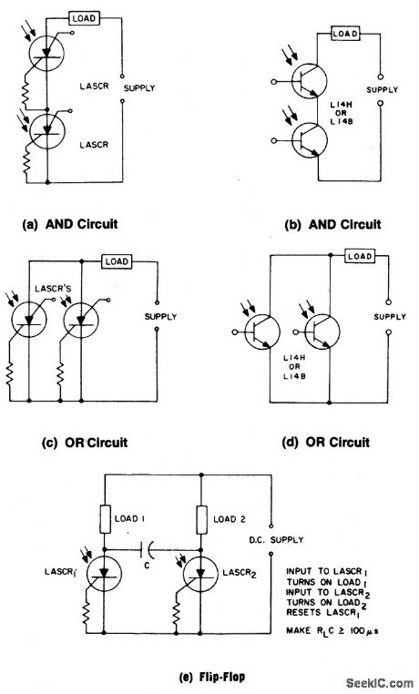
These circuits illustrate some of the common logic functions that can be implemented. (View)
View full Circuit Diagram | Comments | Reading(879)
JFET_PIERCE_CRYSTAL_OSCILLATOR__
Published:2009/6/25 3:04:00 Author:May
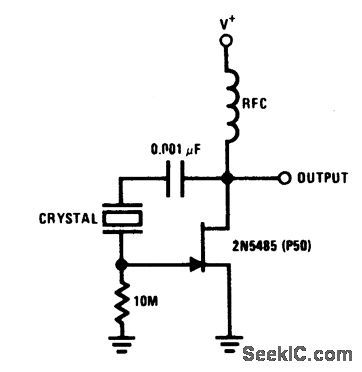
Circuit Notes TheJFET Pierce crystal oscillator allowsa wide frequency range of crystals to be usedwithout circuit modification,Since the JFETgate does not load the crystal, good Q IS maln-tained,thus lnsurlng good frequency stability. (View)
View full Circuit Diagram | Comments | Reading(1159)
STABLE_LOWFREQUENCY_CRYSTAL_OSCILLATOR
Published:2009/6/25 3:02:00 Author:May
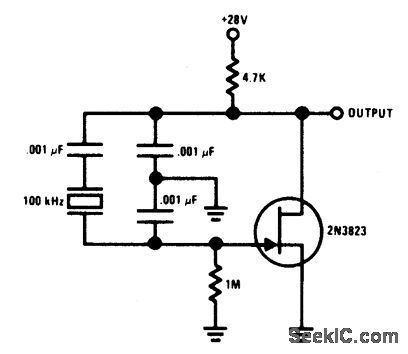
Circuit Notes This Colpitts-crystal oscillator IS ideal forlow frequency crystal oscillator circuits。 Ex-cellent stability is assured because the 2N3823 JFET circuit loading does not vary with tem-perature. (View)
View full Circuit Diagram | Comments | Reading(1134)
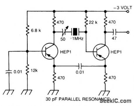
CRYSTAL_CONTROLLED___SINE_WAVE_OSCILLATOR_
Published:2009/6/25 3:00:00 Author:May
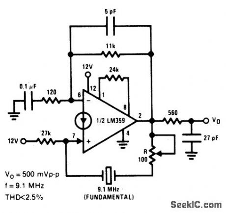
View full Circuit Diagram | Comments | Reading(842)
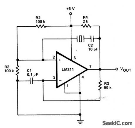
TTL_COMPATIBLE_CRYSTAL_OSCILLATOR
Published:2009/6/25 2:57:00 Author:May
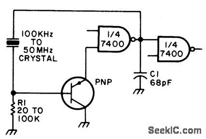
Circuit NotesAdjust RI for about 2 volts at the output ofthe first gate,Adjust C1 for best output (View)
View full Circuit Diagram | Comments | Reading(810)
SINGLE_LTC_POWER_SUPPLY
Published:2009/6/25 2:56:00 Author:May
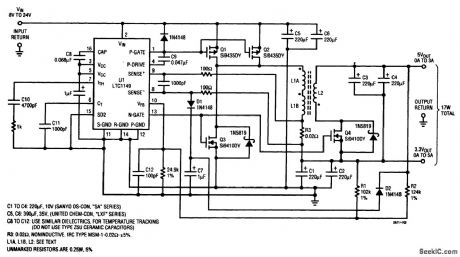
One LTC 1149 synchronous switching regulator can deliver both 3.3- and 5-V outputs. The design's simplicity, low cost, and high efficiency make it a strong contender for portable, battery-powered applications. The circuit described accepts input voltages from 8 to 24 V, to power any combination of 3.3-V and 5-V loads totalling 17 W or less. For input voltages in the 8-V to 16-V range, the LTC1148 may be used, reducing both quiescent current and cost. (View)
View full Circuit Diagram | Comments | Reading(718)
STANDARD_CRYSTALOSCILLATOR_FOR_1_MHz
Published:2009/6/25 2:55:00 Author:May
View full Circuit Diagram | Comments | Reading(621)
INTERNATIONAL_CRYSTAL_OF_1_HI_OSCILLATOR
Published:2009/6/25 2:55:00 Author:May
Circuit NotesInternational Crystal OF-1 HI oscillator circuit for third-overtone crystals. The circuit does not requlre inductors. (View)
View full Circuit Diagram | Comments | Reading(757)
LOW_LEVEL_WARNING_WITH_AUDIO_OUTPUT
Published:2009/6/25 2:53:00 Author:May
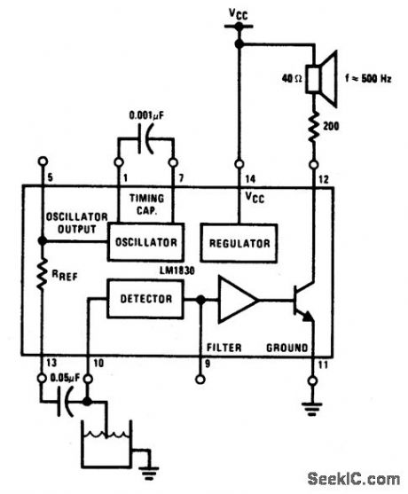
View full Circuit Diagram | Comments | Reading(986)
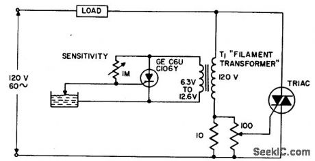
LIQUID_LEVEL_DETECTOR
Published:2009/6/25 2:52:00 Author:May
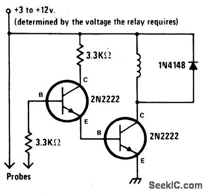
When liquid level reaches both probes, alarm is tumed on. When water level recedes it goes off. (View)
View full Circuit Diagram | Comments | Reading(807)
FLOOD_ALARM
Published:2009/6/25 2:51:00 Author:May
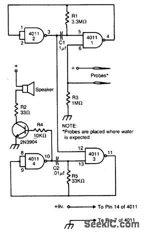
The alarm is built around two audio oscillators, each using two NAND gates. The detection oscillator is gated on by a pair of remote probes. One of the probes is connected to the battery supply, the other to the input of one of the gates. When water flows between the probes, the detection oscillator is gated on.The alarm oscillator is gated on by the output of the detection oscillator. The values given produce an audio tone of about 3000 Hz. The detection oscillator gates this audio tone at a rate of about 3 Hz. The result is a unique pulsating note. Use any 8 ohm speaker to sound the alarm. The 2N3904 can be replaced by any similar NPN transistor. The circuit will work from any six to 12-volt supply. (View)
View full Circuit Diagram | Comments | Reading(3036)
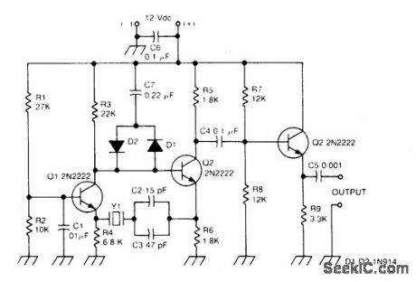
TONE_ALERT_DECODER
Published:2009/6/25 2:51:00 Author:May


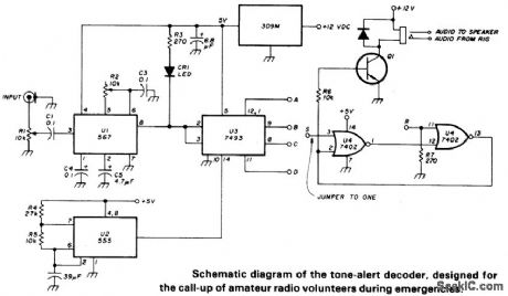

Circuit Notes
PLL (U1) is set with R2 to desired tone frequency. LED lights to indicate lock-up of PLL. Reduce signal level (R1) and readJust R2 to assure lock-up. Delay is selected from counter U3 output. Circuits latches (turns on Q1 to allow audio to speaker) when proper frequency/duration signal is received. To reset latch, a positive voltage must be applied briefly to the R input of U4. (View)
View full Circuit Diagram | Comments | Reading(989)
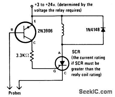
WATER_LEVEL_SENSING_CONTROL_CIRCUIT
Published:2009/6/25 2:50:00 Author:May


The circuit applies power to the load until the water conducts through the probe, and bypasses gate current from the low current SCR. This gives an isolated low voltage probe to satisfy safety requirements. (View)
View full Circuit Diagram | Comments | Reading(770)
BUTLER_APERIODIC_OSCILLATOR
Published:2009/6/25 2:50:00 Author:May
Circuit Notes
This circuit works well in the range of 50 kHz to 500 kHz. Slight component modifica-tions are needed for higher frequency opera-tion. For operation over 3000 kHz, select a transistor that provides moderate gain (in the 60 to 150 range) at the frequency of operation and a gain-bandwidth product of at least 100 MHz. (View)
View full Circuit Diagram | Comments | Reading(685)
WATER_LEVEL_ALARM
Published:2009/6/25 2:49:00 Author:May
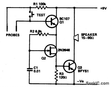
The circuit draws so little current that theshelf-line of the battery is the limiting factor.The only current drawn is the leakage of the transistor. The circuit is shown in the form of awater level alarm but by using different forms of probe can act as a rain alarm or shorting ween the probes will trigger it. Q1 acts as a switch which applies current to the unijunction relaxation oscillator Q2. Alarm signal frequency is controlled by values and ratios of C1/R2. Pulses switch Q3 on and off, applying a signal to the speaker. Almost any NPN silicon transistor can be used for Q1 and Q3 and almost any unijunction for Q2. (View)
View full Circuit Diagram | Comments | Reading(120)
LIQUID_LEVEL_DETECTOR(LATCHING)
Published:2009/6/25 2:48:00 Author:May
Alarm is actuated when liquid level is above the probes and remains activated even if the level drops below the probes. This latching action lets you know that the pre-set level has been reached or exceeded sometime in the past. (View)
View full Circuit Diagram | Comments | Reading(586)
LIQUID_LEVEL_CONTROL
Published:2009/6/25 2:47:00 Author:May
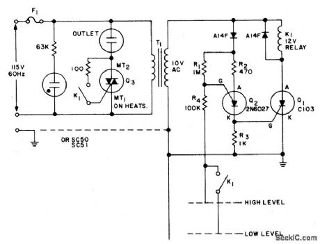
Use this circuit to keep the fluid level of a liquid between two fixed points. Two modes, for filling or emptying are possible by simple reversing the contact connections of K1. The loads can be either electric motors or solenoid operated valves, operating from ac power.Liquid level detection is accomplished by two metal probes, one measuring the high level and the other the low level. An inversion of the logic (keeping the container filled) can be accomplished by replacing the normally open contact on the gate of Q3 with a normally closed contact. (View)
View full Circuit Diagram | Comments | Reading(0)
| Pages:1309/2234 At 2013011302130313041305130613071308130913101311131213131314131513161317131813191320Under 20 |
Circuit Categories
power supply circuit
Amplifier Circuit
Basic Circuit
LED and Light Circuit
Sensor Circuit
Signal Processing
Electrical Equipment Circuit
Control Circuit
Remote Control Circuit
A/D-D/A Converter Circuit
Audio Circuit
Measuring and Test Circuit
Communication Circuit
Computer-Related Circuit
555 Circuit
Automotive Circuit
Repairing Circuit