
Circuit Diagram
Index 1317
PRECISION_PHOTODIODE_LEVEL_DETECTOR
Published:2009/6/24 23:49:00 Author:May
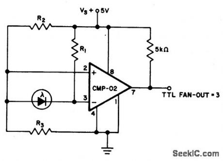
For R1=2.5 M,R2=R3=5 M.The output state changes at a photo diode current of 0.5μA (View)
View full Circuit Diagram | Comments | Reading(697)
LIGHT_ISOLATED_SOLID_STATE_POWER_RELAY_CIRCUITS
Published:2009/6/24 23:48:00 Author:May
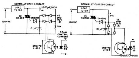
Both circuits use the G.E. SC146B, 200 V, 10 A Triac as load current contacts. These triacs are triggered by normal SBS (2N4992) trigger circuits, which are controlled by the photo-Darlington, acting through the DA806 bridge as an ac photo switch. To operate the relays at other line voltages the asterisked (*) components are scaled to supply identical current. Ratings must be changed as required.Incandescent lamps may be used in place of the light emitting diodes, if desired. (View)
View full Circuit Diagram | Comments | Reading(1728)
NULL_DETECTOR
Published:2009/6/24 23:45:00 Author:May
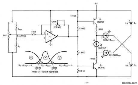
Null detector uses simple LED readout to indicate iftest resistor Rx is below, equal to, or greater than test resistance Rref. If Rx = Rref, the 741 output sits at midpoint value of 4.5 volts and LED A lights. Otherwise, the output of the 741 turns off one transistor and diverts current from the other transistor through B or C, depenging on the polarity of the input voltage difference.Null-detector resoinse is illustrated. (View)
View full Circuit Diagram | Comments | Reading(0)
OPTICAL_RECEIVER
Published:2009/6/24 23:44:00 Author:May
The MFOD1100 PIN diode requires shielding from emi. (View)
View full Circuit Diagram | Comments | Reading(0)
555_OSCILLATOR_FOR_DRIVING_A_PIEZO_TRANSDUCER
Published:2009/6/24 23:44:00 Author:May
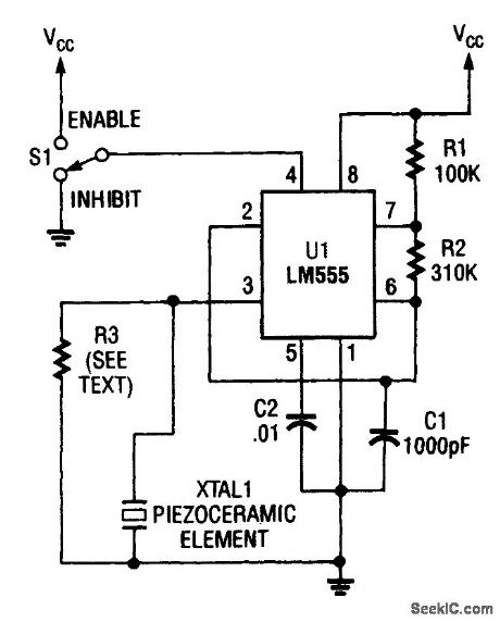
A 555-timer oscillator is perhaps one of the most popular circuits for driving a piezoelectric transducer. (View)
View full Circuit Diagram | Comments | Reading(3234)
LIGHT_INTERRUPTION_DETECTOR
Published:2009/6/24 23:44:00 Author:May
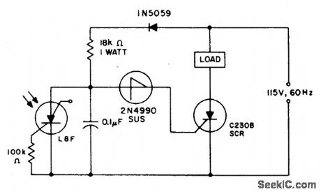
When the light incident on the LASCR is interrupted, the voltage at the anode to the 2N4990 unilateral switch goes positive on the next positive cycle of the power which in turn triggers the switch and the C230 SCR when the switching voltage of the unilateral switch is reached. This will cause the load to be energized for as long as light is not incident on the LASCR. (View)
View full Circuit Diagram | Comments | Reading(1623)
PIEZO_MICROPOSITIONER_DRIVER
Published:2009/6/24 23:43:00 Author:May
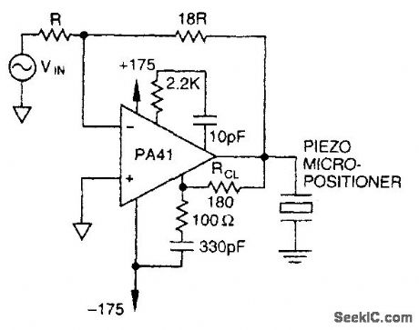
The PA41 from Apex Microtechnology is used here to drive a piezoelectric micropositioner. The drive voltage is less than 20 V p-p at input. (View)
View full Circuit Diagram | Comments | Reading(786)
OPTICAL_TRANSMITTER
Published:2009/6/24 23:43:00 Author:May
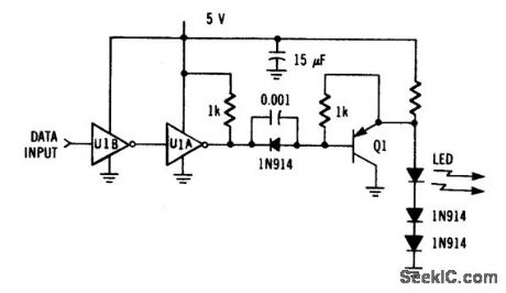
Driver circuit uses an MC74LS04 and one discrete transistor. The circuit can drive the LED (MFOE1200) at up to 1 Mbps data rate. (View)
View full Circuit Diagram | Comments | Reading(0)
PIEZO_DRIVER
Published:2009/6/24 23:42:00 Author:May
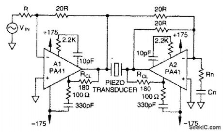
Using a PA41 from Apex Microtechnology, this monolithic amplifier is capable of 350-V operation and delivers 660 V p-p in a bridge circuit. (View)
View full Circuit Diagram | Comments | Reading(1621)
IMPEDANCE_CONVERTER
Published:2009/6/24 23:42:00 Author:May
Used to match 10-megohrninputimpedanceto 50-ohm transmission Iine or 50-ohm input of instruments such as spectrum analyzer, video amplifier, or fre-quency counter. Voltage gain is exactly 0.5. Fre-quency response is from DC to 20 MHz and can be boosted by using higher-frequency transis-tor.-M. J. Salvati, FET Probe Drives 50-Ohm Load, EDN Magazine, March 5, 1973, p 87 and 89. (View)
View full Circuit Diagram | Comments | Reading(0)
PHOTOCELL_MEMORY_SWITCH_FOR_AC_POWER_CONTROL
Published:2009/6/24 23:42:00 Author:May
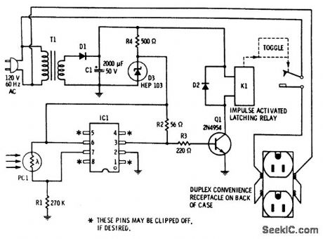
Provides remote control for ac-powered devices by using the beam of a flashlight as a magic wand. The important aspect of this gadget is that it remembers. Activate it once to apply power to a device and it stays on. Activate it a second time and power goes off and stays off. It consists of a combination of a high-sensitivity photocell, a highgain IC Schmitt trigger, and an impulse-actuated latching relay. (View)
View full Circuit Diagram | Comments | Reading(0)
MULTIPURPOSE_MODULE
Published:2009/6/24 23:41:00 Author:May
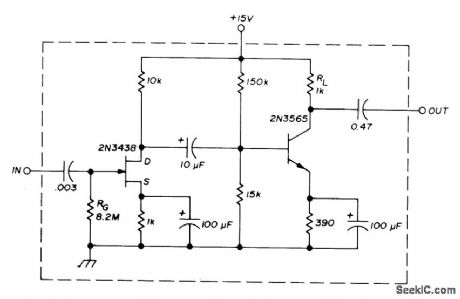
Flexible circuit using FET to drive bipolar transistor has -3 dB points at 100 Hz and 0.6 MHz. Components are noncritical and can be changed considerably in value to optimize gain, frequency response, power output, or power consumption. Load presented to FET is primarily input resistance of bipolar transistor, about 1000 ohms, which gives voltage gain of 4 for FET.-I. M Gottlieb, A New Look at Solid-State Amplifiers, Ham Radio, Feb. 1976, p 16-19. (View)
View full Circuit Diagram | Comments | Reading(0)
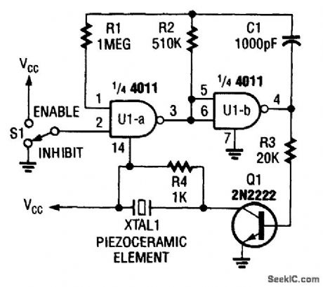
CMOS_PIEZO_DRIVER_USING_4049
Published:2009/6/24 23:41:00 Author:May

This circuit uses a 4049 IC to drive a 2N2222 switching transistor The transistor drives crysbal 1 a ptezo transducer. (View)
View full Circuit Diagram | Comments | Reading(2671)
CMOS_PIEZO_DRIVER
Published:2009/6/24 23:39:00 Author:May
A CMOS-gate and transistor buffer can be used as an effective driver for a piezoelectric transducer. (View)
View full Circuit Diagram | Comments | Reading(1375)
ENLARGER_EXPOSURE_METER
Published:2009/6/24 23:36:00 Author:May
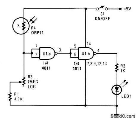
Two gates of a 4011 are used as a comparator. When the resistance of R4 decreases the voltage at pin 1 and 2 increases, producing a logic zero at pin 3, causing pin 4 to go high and activating the LED. R3 is calibrated in light units, or seconds exposure time. To calibrate, set pot R3 so as to just be on the LED ON/OFF threshold. With a light level that is suitable to correctly expose a photographic print, use a known enlarger and a known negative. (View)
View full Circuit Diagram | Comments | Reading(0)
PARAPHASE_PHASE_INVERTER
Published:2009/6/24 23:34:00 Author:May

Uses 180° phase difference between source and drain out-puts of Siliconix Ut83 FET to convert AF input to push-pull output without transformer. Volt-age gain in each half of circuit is about 0.8. Frequency response referred to 1 kHz is flat within 3 dB from 50 Hz to 50 kHz, when using lmeg-ohm output load.-R. P. Turner, FET Circuits, Howard VV. Sams, Indianapolis, IN, 1977, 2nd Ed.,p 29-30. (View)
View full Circuit Diagram | Comments | Reading(0)
OPTICAL_TRANSMITTER
Published:2009/6/24 23:43:00 Author:Jessie
Driver circuit uses an MC74LS04 and one discrete transistor. The circuit can drive the LED (MFOE1200) at up to 1 Mbps data rate. (View)
View full Circuit Diagram | Comments | Reading(1526)
STROBE_LIGHT
Published:2009/6/24 23:34:00 Author:May
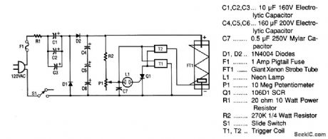
This strobe light operates from standard 120-Vac power,R1 limits the amount of current applied to the voltage doubler stage,which is comprtsed of C1,C2,C3,D1,D2,C4,C5,and C6 Capacitors C1,C2,and C3 are connected in parallel and form a capacitance of 30 μF at 160V. Capacitors C4, C5, and C6 are connected in serles and form an equivalent capacitor of about 53 μF at 480 V . Diodes D1 and D2 not only rectify the ac voltage,but also complete the vltage doubler stage,which convertsthe incoming 120 Vac to the appropriately 300 V that are required by the xenon strobe tube.
The next stage of the circuit is the neon relaxation oscillator and trigger stage This stage is made up of R2, P1,C7,L1,Q1,T1,and T2.As the storage capacitor (made up of C4,C5,and C6) reaches its full-capaclty charge,the voltage divider (made up of R2 and P1) applies voltage to capacitor C7. As C7 charges up,it reaches a threshold voltage level,SCR Q1. When Q1 has a positive pulse on its gate,it fires(causes a short from anode to cathode). That firing action discharges most of the energy stored in C7 into trigger transformers T1 and T2(which have secondaries connected in series to developer 8 kV). The frequency of the 8-kV pulses is determined by the setting of P1 and the value of C7. Because C7 is a fixed capacitor,only the Setting of P1 adjusts the flash rate in this circuit
As soon as an 8-kV pulse is applied from the secondary of T2 (trigger wire) to the trigger lead of FT1,it discharges storage capacitors C4,C5,and C6,which causes it to ionize (flash). The cycle thenrepeats itself until the power is removed from the circuit board by turning off S1 or removing the line cord. (View)
View full Circuit Diagram | Comments | Reading(3304)
PIEZO_DRIVER
Published:2009/6/24 23:42:00 Author:Jessie
Using a PA41 from Apex Microtechnology, this monolithic amplifier is capable of 350-V operation and delivers 660 V p-p in a bridge circuit. (View)
View full Circuit Diagram | Comments | Reading(0)
500_kHz_TO_500_MHz
Published:2009/6/24 23:34:00 Author:May
Two-stage general-pur-pose wideband small-signal amplifier provides nearly 14-dB gain at 150 MHz when inserted in 50-ohm transmission line with no tuned circuits at input or output. Noise figure with optimum source resistance is about 3 dB at 150 MHz. Am-plifier is capaeitively coupled common-emitter cascade. Capacitors make low-frequency gain begin dropping off below about 2 MHz. Increas-ing all capacitors to 0.01μF will lowerfrequency response to about 200 kHz.-R. Rhea, General Purpose Wideband RF Amplifier, Ham Radio, April 1975, p 58-61. (View)
View full Circuit Diagram | Comments | Reading(1162)
| Pages:1317/2234 At 2013011302130313041305130613071308130913101311131213131314131513161317131813191320Under 20 |
Circuit Categories
power supply circuit
Amplifier Circuit
Basic Circuit
LED and Light Circuit
Sensor Circuit
Signal Processing
Electrical Equipment Circuit
Control Circuit
Remote Control Circuit
A/D-D/A Converter Circuit
Audio Circuit
Measuring and Test Circuit
Communication Circuit
Computer-Related Circuit
555 Circuit
Automotive Circuit
Repairing Circuit