
Circuit Diagram
Index 1319
23O_W_WATER_COOLED
Published:2009/6/24 23:35:00 Author:Jessie
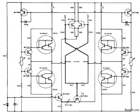
Used to excite mag-netic specimens in frequency range of 0 to 110 kHz at outputs up to 12 A. Output stage uses two complementary pairs of emitter-followers connected so each pair forms half of bridge, using MJ4030 and MJ4033 Darlingtons mounted on Iiquid-cooled heatsinks. Article describes cooling arrangement and circuit opera-tion in detail and gives suitable preamp circuit for driving inputs of BCY89 dual transistor. De-signed for 32-VDC supply, which connects to top and bottom horizontal buses on diagram.Feedback circuit are drawn in heavy lines. Re-sistors in series with Darlingtons (OR25, representing 0.25 ohm) are wound from resistance wire since they must carry large currents. Output impedance of circuit is less than 0.5 ohm, for matching to low-resistance load.-I. L. Ste-fani and II. Perryman, Liquid-Cooled Power Am-plifier, Wireless World, Dec. 1974, p 505-507. (View)
View full Circuit Diagram | Comments | Reading(804)
PARAPHASE_PHASE_INVERTER
Published:2009/6/24 23:34:00 Author:Jessie

Uses 180° phase difference between source and drain out-puts of Siliconix Ut83 FET to convert AF input to push-pull output without transformer. Volt-age gain in each half of circuit is about 0.8. Frequency response referred to 1 kHz is flat within 3 dB from 50 Hz to 50 kHz, when using lmeg-ohm output load.-R. P. Turner, FET Circuits, Howard VV. Sams, Indianapolis, IN, 1977, 2nd Ed.,p 29-30. (View)
View full Circuit Diagram | Comments | Reading(2274)
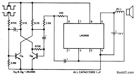
CARRIER_CURRENT_TRANSMITTER
Published:2009/6/24 23:24:00 Author:May
View full Circuit Diagram | Comments | Reading(0)
STROBE_LIGHT
Published:2009/6/24 23:34:00 Author:Jessie
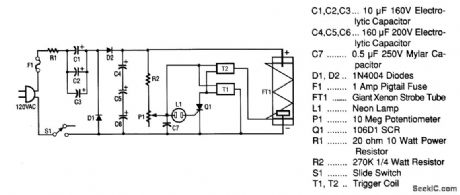
This strobe light operates from standard 120-Vac power,R1 limits the amount of current applied to the voltage doubler stage,which is comprtsed of C1,C2,C3,D1,D2,C4,C5,and C6 Capacitors C1,C2,and C3 are connected in parallel and form a capacitance of 30 μF at 160V. Capacitors C4, C5, and C6 are connected in serles and form an equivalent capacitor of about 53 μF at 480 V . Diodes D1 and D2 not only rectify the ac voltage,but also complete the vltage doubler stage,which convertsthe incoming 120 Vac to the appropriately 300 V that are required by the xenon strobe tube.
The next stage of the circuit is the neon relaxation oscillator and trigger stage This stage is made up of R2, P1,C7,L1,Q1,T1,and T2.As the storage capacitor (made up of C4,C5,and C6) reaches its full-capaclty charge,the voltage divider (made up of R2 and P1) applies voltage to capacitor C7. As C7 charges up,it reaches a threshold voltage level,SCR Q1. When Q1 has a positive pulse on its gate,it fires(causes a short from anode to cathode). That firing action discharges most of the energy stored in C7 into trigger transformers T1 and T2(which have secondaries connected in series to developer 8 kV). The frequency of the 8-kV pulses is determined by the setting of P1 and the value of C7. Because C7 is a fixed capacitor,only the Setting of P1 adjusts the flash rate in this circuit
As soon as an 8-kV pulse is applied from the secondary of T2 (trigger wire) to the trigger lead of FT1,it discharges storage capacitors C4,C5,and C6,which causes it to ionize (flash). The cycle thenrepeats itself until the power is removed from the circuit board by turning off S1 or removing the line cord. (View)
View full Circuit Diagram | Comments | Reading(0)
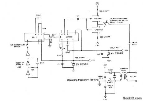
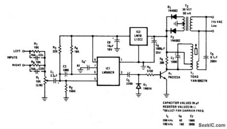
CARRIER_CURRENT_RECEIVER
Published:2009/6/24 23:21:00 Author:May
160 kHz transformer consists of a 18 x 11mm ungapped pot core (Siemens, Ferrocube, etc.), itilizing magnerics incorporated type F material wond woth 80 1/2 turns of No.35 sire for the secondary and 5 1/2 turns for the primary. This gives a turns ratio fo approximately 15 to 1. (View)
View full Circuit Diagram | Comments | Reading(0)
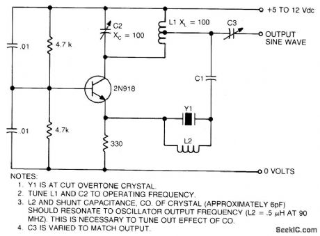
OVERTONE_OSCILLATOR_WITH_CRYSTAL_SWITCHING
Published:2009/6/24 23:18:00 Author:May
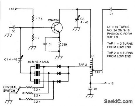
Circuit Notes
The large inductive phase shift of L1 is compensated for by C1. Overtone crystals have very narrow bandwidth; therefore, the trimmer has a smaller effect than for fundamental-mode operation. (View)
View full Circuit Diagram | Comments | Reading(0)
200_kHz_LINE_CARRIER_TRANSMITTER_WITH_ON_OFF_CARRIER_MODULATOR
Published:2009/6/24 23:16:00 Author:May
View full Circuit Diagram | Comments | Reading(0)
PHOTO_STROBE_SLAVE_TRIGGER
Published:2009/6/24 23:14:00 Author:May
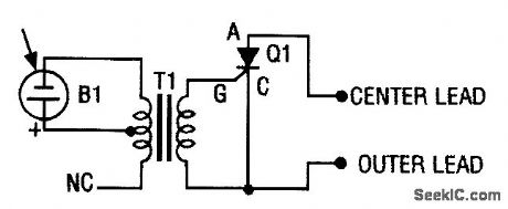
The photo strobe slave trigger circuit uses a solar cell and an SCR to flash any strobe when you trigger your master strobe. The tiny solar cell produces a vet'y small voltage when light falls on its surface. (View)
View full Circuit Diagram | Comments | Reading(0)
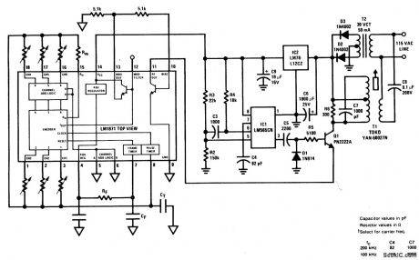
Carrier_System_Transmitter
Published:2009/6/24 23:14:00 Author:May
High quality, noise free, wireless FM transmitter/receiver operates over standard power lines. Complete system is suitable for high-quality transmission of speech or music, and will operate from any ac outlet anywhere on a one-acre homesite. Frequency response is 20-20, 000 Hz and THD is under 1/2%. Transmission distance along a power line is at least adequate to include all outlets in and around a suburban home and yard.Two input terminals are provided so that both left and right signals of a stereo set may be combined for mono transmission to a single remote speaker if desired. (View)
View full Circuit Diagram | Comments | Reading(0)
DARKROOM_TIMER
Published:2009/6/24 23:13:00 Author:May
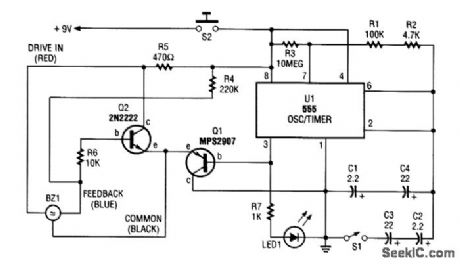
The electronic darkroom timer is built around a 555 oscillator/timer, a pair of general-purpose transistors, a buzzer, and an LED. The 555 (U1) is configured as an astable multivibrator (free-rututing oscillator). The frequency of the oscillator is determined by the values R1 through R3 and C1 through C4.
Switch S1 is used to divide the capacitor network to vary the time interval between beeps; when S1 is closed, the circuit beeps at intervals of 30 seconds. With S1 closed, it beeps at 15-second intervals.
When power is applied to the circuit (by closing switch S2), the output of U1 at pin 3 is initially high. That high is applied to the base of transistor Q1 (an MPS2907 general-purpose pnp device), keeping it turned off. That high is also applied to the anode of LED1 (which is used as a power on indicator) through resistor R7, turning it on.
Timing capacitors C1 through C5 begin to charge through timing resistors R1 through R3. dc voltage is applied to BZ1's driver input through R5 and to its feedback terminal (through R4), which is also connected to Q2's base terminal. The V+ voltage that applied to Q2's base causes it to turn on, tying BZ1's common terminal high.
When the timing capacitors are sufficiently charged, a trigger pulse is applied to pin 2 (the trigger input) of U2, causing U1's output to momentarily go low. This causes LED1 to go out and tran-sistor Q1 to turn on. That, in turn, grounds the common lead of buzzer BZ1, causing BZ1 to sound. Afterward, the output of U1 returns to the high state, turning off Q1, and turning on LED1, until another time interval has elapsed and the process is repeated.
The circuit is powered by a 9-Vac adapter, which plugs into a standard 117-V household outlet. Because the circuit draws only about 10 to 15 mA, a 9-V alkaline transistor-radio-battery can also be used to power the circuit. (View)
View full Circuit Diagram | Comments | Reading(0)
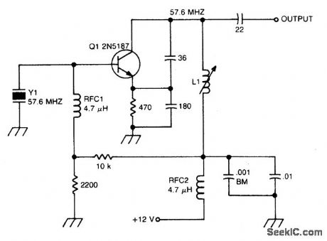
CRYSTAL_CONTROLLED_BUTLER_OSCILLATOR
Published:2009/6/24 23:13:00 Author:May
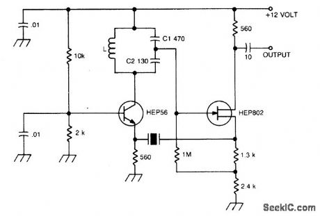
Circuit NotcsA typical Butler oscillator (20-100 MHz) uses an FET in the second stage; the circuit is not reliable with two bipolars. Sometimes two FETs are used. Frequency is determined by LC values. (View)
View full Circuit Diagram | Comments | Reading(0)
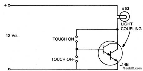
LATCHING,DOUBLE_BUTTON_TOUCH_SWITCH
Published:2009/6/24 23:11:00 Author:May
View full Circuit Diagram | Comments | Reading(0)
CMOS_TOUCH_SWITCH
Published:2009/6/24 23:10:00 Author:May
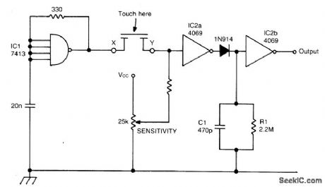
This touch switch does not rely on mains hum for switching. It can be used with battery powered circuits. Schmitt trigger IC1 forms a I 100 kHz oscillator and IC2a which is biased into the linear region, amplifies the output and charges C1 via the diode. IC2b acts as a level detector. When the sensor is touched, the os-cillator signal is severely attenuated which causes C1 to discharge and IC2b to change state. (View)
View full Circuit Diagram | Comments | Reading(0)
TOUCH_CIRCUIT
Published:2009/6/24 23:10:00 Author:May
View full Circuit Diagram | Comments | Reading(0)
PTOXIMITY_DETECTOR
Published:2009/6/24 23:09:00 Author:May
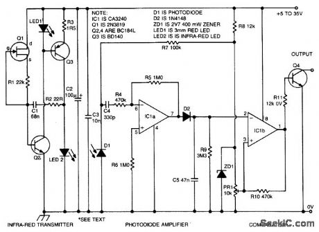
The proximity sensor works on the principle of transmitting a beam of modulated infra-red light from the emitter diode LED2, and receiving reflections from objects passing in front of the beam with a photodiode detector D1. The circuit can be split into three distinct stages; the infra-red transmitter, the photodiode amplofoer, and a variable threshol comparator. (View)
View full Circuit Diagram | Comments | Reading(0)
FIFTH_OVERTONE_OSCILLATOR
Published:2009/6/24 23:06:00 Author:May
Circuit NotesThis circuit isolates the crystal from the dc base supply with an rf choke for better starting characteristics. (View)
View full Circuit Diagram | Comments | Reading(0)
TOUCH_SWOTCH_OR_PROXIMITY_DETECTOR
Published:2009/6/24 23:04:00 Author:May
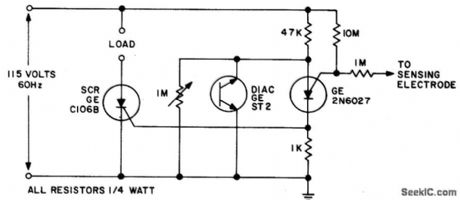
This circuit is actuated by an increase in capacitance between a sensing electrode and the ground side of the line. The sensitivity can be adjusted to switch when a human body is within inches of the insulated plate used as the sensing electrode. Thus, sensitivity is adjusted with the 1 megohm potentiometer which de-termines the anode voltage level prior to clamping. This sensitivity will be proportional to the area of the surface opposing each other. (View)
View full Circuit Diagram | Comments | Reading(0)
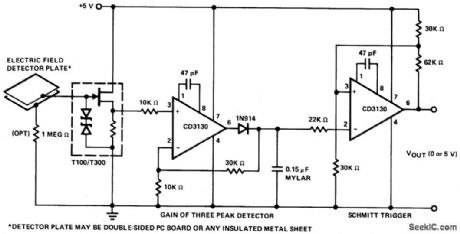
SELF_BIASED_PROXIMITY_SENSOR_WORKS_ON_DETECTED_CHANGING_FIELD
Published:2009/6/24 23:03:00 Author:May
View full Circuit Diagram | Comments | Reading(1639)
50_MHz_150_MHz_OVERTONE_OSCILLATOR
Published:2009/6/24 23:02:00 Author:May
View full Circuit Diagram | Comments | Reading(0)
CAPACITANCE_OPERATED_ALARM_TO_FOIL_PURSE_SNATCHERS
Published:2009/6/24 23:01:00 Author:May
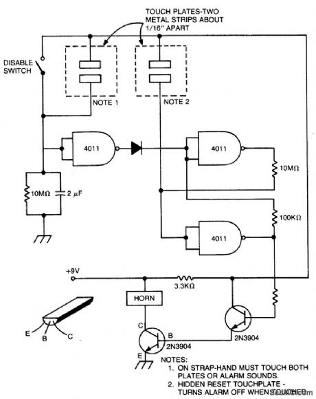
Aslong as touch plates (1) are touched together,the alarm is off. If not held for about 30 seconds,the alarm goes off. The circuit can be disabled with switch or by touching the plates (2),The alarm is battery operated by a bicycle horn. (View)
View full Circuit Diagram | Comments | Reading(0)
| Pages:1319/2234 At 2013011302130313041305130613071308130913101311131213131314131513161317131813191320Under 20 |
Circuit Categories
power supply circuit
Amplifier Circuit
Basic Circuit
LED and Light Circuit
Sensor Circuit
Signal Processing
Electrical Equipment Circuit
Control Circuit
Remote Control Circuit
A/D-D/A Converter Circuit
Audio Circuit
Measuring and Test Circuit
Communication Circuit
Computer-Related Circuit
555 Circuit
Automotive Circuit
Repairing Circuit