
Circuit Diagram
Index 1300
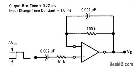
POSITIVE_EDGE_DIFFERENTIATOR
Published:2009/6/25 21:19:00 Author:May
View full Circuit Diagram | Comments | Reading(0)
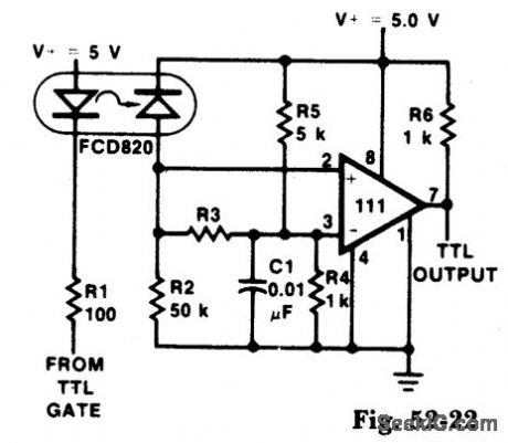
DIGITAL_TRANSMISSION_ISOLATOR
Published:2009/6/25 21:29:00 Author:Jessie
View full Circuit Diagram | Comments | Reading(1555)
SOUND_ACTIVATED_RELAY
Published:2009/6/25 21:19:00 Author:May
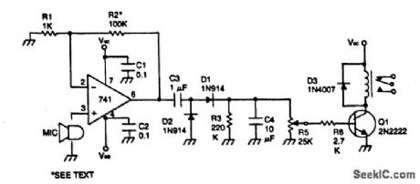
The device remains dormat (in an off con-dition) until some sound causes it to turn on. The input stage is a 741 operational amplifier connected as a noninverting follower audio amplifier. Gain is approximately 100. To increase gain raise the value of R2. The amplified signal is rectified and filtered to a dc level by R4. Then R5 is set to the audio level desired to activate the relay. (View)
View full Circuit Diagram | Comments | Reading(909)
STYLUS_ORGAN
Published:2009/6/25 21:18:00 Author:May
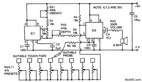
IC2 is an audio frequency oscillator. Its frequency is primarily controlled by the resistance between pins 2 and 7. RV4-11 control the oscillator frequency and by touching a stylus (connected via limiting resistor R5 to pin 2) to each preset, different notes can be played. IC1 is a low frequency oscillator (approximately 3-10Hz), the frequency of which is variable by RV1. The output of this oscillator is connected through depth control RV2 and limiting resistor R3 to the voltage control input of the audio frequency oscillator. Thus a vibrato effect occurs. (View)
View full Circuit Diagram | Comments | Reading(818)
10_dB_GAIN_AT_001_1OO_MHz
Published:2009/6/25 21:17:00 Author:May
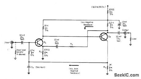
High-gain wideband untuned general-purpose amplifier uses Fairchild 2N5126 or equivalent transistors in direct-coupled circuit. Design is stable for both power supply and temperature variations.Gain is adjusted with R1, with maximum of 38 to 44 dB and maximum output of about 1V P-P.Will drive low-level transistor circuits having load of about 1000 ohms. If several amplifiers are used in series for higher gain, shielding is required. Applications include amplification of pulsed light signals detected by photodiode. Cx can be 100-pF mica,-A. B Hutchison, Jr., Gen-eral Purpose Wide Band Amplifier, CQ, May 1972, p 22-23. (View)
View full Circuit Diagram | Comments | Reading(854)
AUDIO_CONTROLLED_LAMP
Published:2009/6/25 21:17:00 Author:May
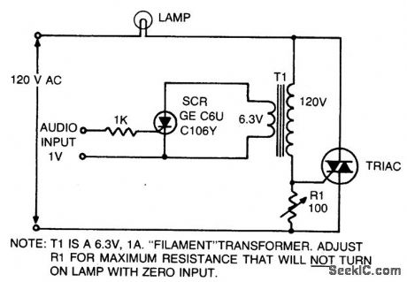
This is an on-off control with isolated, low voltage input. Since the switching action is very rapid, compared with the response time of the lamp and the response of the eye, the effect produced with audio input is similar to a pro-portional control circuit. If the input signal to the SCR consists of phase-controlled pulses, full wave control of the lamp load is obtained. (View)
View full Circuit Diagram | Comments | Reading(808)
DIFFERENTIATOR_WITH_HIGH_COMMON_MODE_NOISE_REJECTION_
Published:2009/6/25 21:28:00 Author:Jessie
View full Circuit Diagram | Comments | Reading(1155)
HIGH_Z_PREAMP
Published:2009/6/25 21:16:00 Author:May
Provides up to 20 megohms of input impedance and has essentially flat response from 10 Hz to 220 MHz Q3 serves as emitter resistorfor Q2、and emitter-follower Q4 reduces loading Input impedance is further increased by adding optionalcomponents shownin dashed lines, Transistors are 2N2188,SK3005,GE-9、or HEP-2.-Circuits, 73 Magazlne,Feb,1974、p102. (View)
View full Circuit Diagram | Comments | Reading(907)
SOUND_MODULATED_LIGHT_SOURCE
Published:2009/6/25 21:16:00 Author:May
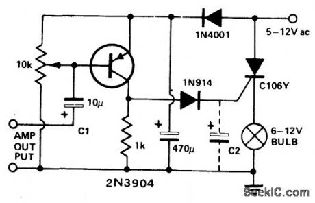
This circuit modulates a light beam with voice or music from the output of an amplifier. If the 10 K pot is adjusted to slightly less than the Vbe of the transistor, the circuit forms a peak detector. This drives the gate of the SCR, lighting the bulb whose brightness will vary as the sound level varies. C2 may be removed for a faster response. (View)
View full Circuit Diagram | Comments | Reading(832)
LOW_DRIFT_INTEGRQTOR_AND_LOW_LEAKAGE_GUARDED_RESET
Published:2009/6/25 21:27:00 Author:Jessie
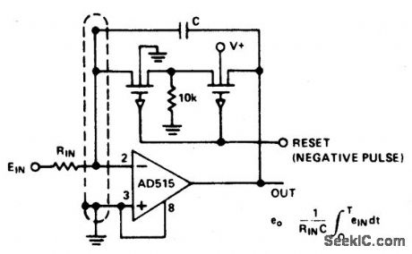
View full Circuit Diagram | Comments | Reading(582)
SQUARE_WAVE_OSCILLATOT
Published:2009/6/25 21:26:00 Author:Jessie
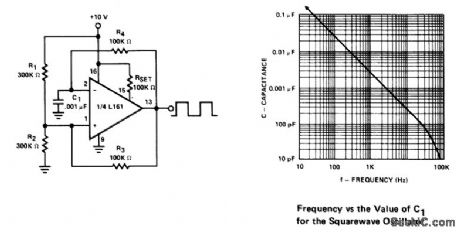
This generator is operable to over 100 kHz. The low frequency limit is determined by C1. Frequency is constant for supply voltages down to +5 V. (View)
View full Circuit Diagram | Comments | Reading(578)
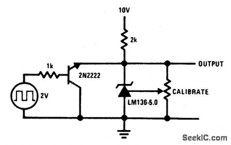
50_V_SQUARE_WAVE_CALLBRATOR
Published:2009/6/25 21:26:00 Author:Jessie
View full Circuit Diagram | Comments | Reading(512)
NEGATIVE_EDGE_DIFFERENTIATOR
Published:2009/6/25 21:16:00 Author:May

View full Circuit Diagram | Comments | Reading(0)
AIR_MOTION_DETECTOR
Published:2009/6/25 21:23:00 Author:Jessie
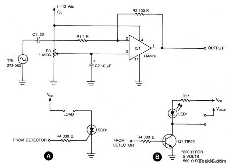
Circuit NotesSensing circuit detects either steady or fluctuating air flows. The heart of the circuit is a Radio Shack piezo buzzer (P/N 273-060) and an LM324 quad op amp. (Red wire from the piezo element connects to capacitor C1, and the black wire to ground.) When a current of air hits the piezo element, a small signal is gener-ated and is fed through C1 and RI to the in-verting input (pin 2) of one section of the LM324. That causes the output (pin 1) to go high. Resistor R3 adjusts sensitivity. The circuit can be made sensitive enough to detect the wave of a hand or the sensitivity can be set so low that blowing on the element hard will pro-duce no output. Resistor R2 is used to adjust the level of the output voltage at pin 1. The detector circuit can be used in various control applications. For example, an SCR can be used to control 117-volt AC loads as shown in A. Also, an NPN transistor, such as a TlP29, can be used to control loads as shown in B. (View)
View full Circuit Diagram | Comments | Reading(2506)
FAST_INVERTER_CIRCUIT
Published:2009/6/25 21:24:00 Author:Jessie
View full Circuit Diagram | Comments | Reading(588)
PRECISION_RECTIFIERS
Published:2009/6/25 21:23:00 Author:Jessie
View full Circuit Diagram | Comments | Reading(555)
AUDIO_OPERATED_RELAY
Published:2009/6/25 21:15:00 Author:May
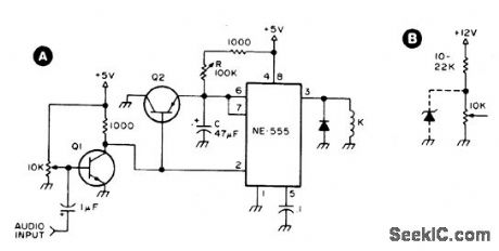
Q1 and Q2 are general purpose transis-tors. The 10 K input pot is adjusted to a point just short of where Q1 turns on as indicated by K pulling in. K is any 5 V reed relay. With the values shown for R (100 K) and C (47 μF), timing values from.05 to slightly over 5 sec-onds can be achieved. B shows the addition o f a 22 K series resistor to the 10 K input pot if a 12 V supply is used. A suitable 12 V reed relay must be used at K. (View)
View full Circuit Diagram | Comments | Reading(0)
LONG_DURATION_TIME_DELAY
Published:2009/6/25 21:14:00 Author:May
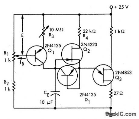
View full Circuit Diagram | Comments | Reading(0)
SHIFT_REGISTER_DRIVER
Published:2009/6/25 21:14:00 Author:May
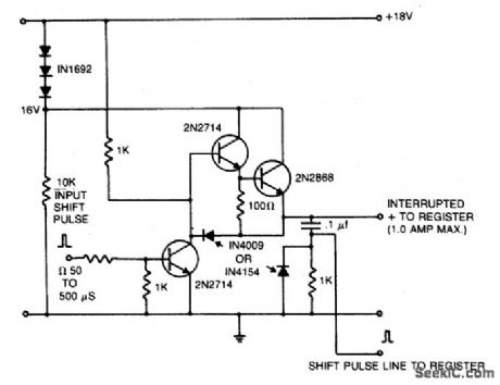
A 16 V power supply can be synthesized as shown using IN1692 rectifiers. A shift pulse input saturates the 2N2714 depriving the Darlington combination (2N2714 and 2N2868) of base drive. The negative pulse so generated on the 15 V line is differentiated to produce a positive trigger pulse at its trailing edge. (View)
View full Circuit Diagram | Comments | Reading(0)
WIDEBAND_VARIABLE_GAIN
Published:2009/6/25 21:14:00 Author:May
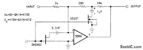
FET selves as ourPur gain-controlled device in feedback loop of Optical Electronics 9906 opamp. Resistive T network has SD201 MOS transistor as ground leg, with resistor values dlosen so transistor is electrically dose to summing junction, automatically limiting total signal voltage. Resulting arrangement of voltage-controlled feedback and compensation gives variable-gain amplifier whh good linearity and constant wideband width for all gain Ievels.- Wideband Variable Gain Amplifier, Optical Electronics, Tucson, AZ, Application Tip 10277. (View)
View full Circuit Diagram | Comments | Reading(0)
| Pages:1300/2234 At 2012811282128312841285128612871288128912901291129212931294129512961297129812991300Under 20 |
Circuit Categories
power supply circuit
Amplifier Circuit
Basic Circuit
LED and Light Circuit
Sensor Circuit
Signal Processing
Electrical Equipment Circuit
Control Circuit
Remote Control Circuit
A/D-D/A Converter Circuit
Audio Circuit
Measuring and Test Circuit
Communication Circuit
Computer-Related Circuit
555 Circuit
Automotive Circuit
Repairing Circuit