
Circuit Diagram
Index 1298
STEREO_BALANCER
Published:2009/6/25 21:46:00 Author:May
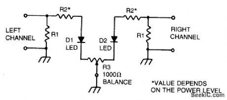
This circuit will allow you to set the gain of two stereo channels to the same level. The signal across the two channel-load resistors is sampled by resistors R2. (Values of these re-sistors will depend upon the power leveL) For most 20 milliampere LED, use approximately 2.5 K per watt. (For a 10-watt system use a 25,000 ohm resistor.) To set up, short the two inputs and connect them to one channel of a power amplifier. Apply a signal and adjust R3 until both LEDs glow at the same brightness level. The balancer is ready for use. Connect the inputs of the stereo balancer across the output of the power amplifier, and then turn up either the independent volume controls, or the balance control until both LEDs glow at the same level. To use this circuit in-line with loudspeakers, disconnect both R1s, and use the speakers as the load. (View)
View full Circuit Diagram | Comments | Reading(853)
CB_MODULATION_MONITOR
Published:2009/6/25 21:48:00 Author:Jessie
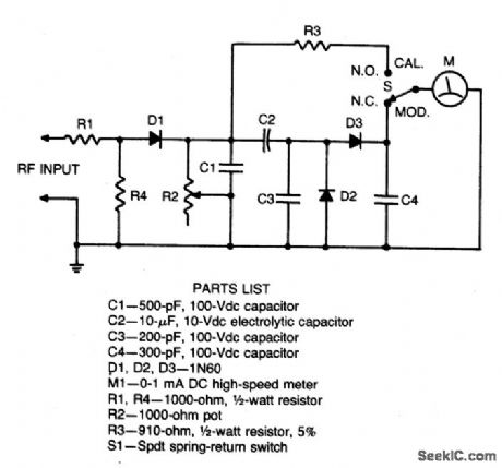
Connect this circuit to a transceiver with a coaxial T connector in the transmission line. Key the transmitter (unmodulated), set S1 to CAL, and adjust R2 for a full scale reading. Return S1 to MOD position. The meter will read % modulation with 10% accuracy. (View)
View full Circuit Diagram | Comments | Reading(1446)
VISUAL_MODULATION_INDICATOR
Published:2009/6/25 21:45:00 Author:May
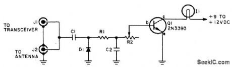
Indicator lamp brightness varies in step with modulated RF signal. Adjust R2 with transmitter on (modulated) until the lamp flashes in step with modulation. C1 = 5 pf, C2 = 100 pF, D1 = 1N60 or 1N34 (Germanium), R3 = 10 K pot, I1 = 6-8 V, 30-60 mA incandes-cent bulb, Q1 = 2N3393 (for increased sensitivity use 2N3392 or other high-gain transistor). (View)
View full Circuit Diagram | Comments | Reading(982)
CONSTANT_OUTPUT_IMPEDANCE
Published:2009/6/25 21:47:00 Author:Jessie
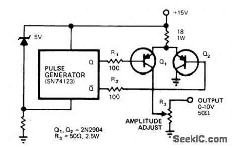
Pulse output stage gives output range from millivolts to 10 V P-P across 50 ohms while optimizing waveform characteristics of output pulse. With 2N2904 output transistors, circuit delivers 200 mA with 20-ms rise and fall times.-W. A. Palm, Pulse Amplifier Varies Amplitude, EDN Maga-zine, Aug. 5, 1978, p 76. (View)
View full Circuit Diagram | Comments | Reading(1147)
LOW_VOLTAGE_DETECTOR
Published:2009/6/25 21:34:00 Author:May
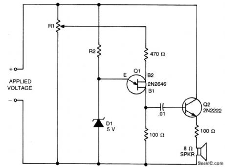
Circuit Notes
The values of R1, R2, and D1 are selected for the voltage applied. Using a 12-volt battery, R1= 10K, R2 = 5.6 K and Di is a 5-volt zener diode, or a string of forward-biased silicon rectifiers equaling about 5 volts. Transistor Q1 is a general-purpose UJT (Unijunction Transis-tor), and Q2 is any small-signal or switching NPN transistor. When detector is connected across the battery terminals, it draws little current and does not interfere with other devices powered by the battery. If voltage drops below the trip voltage selected with the R1 setting, the speaker beeps a waming. The fre-quency of the beeps is determined by the amount of undervoltage. If other voltages are being monitored, select R1 so that it draws only 1 mA or 2 mA. Zener diode D1 is about one-half of the desired trip voltage, and R2 is selected to bias it about 1 mA. (View)
View full Circuit Diagram | Comments | Reading(1631)
CMOS_OSCILLATOR
Published:2009/6/25 21:34:00 Author:May
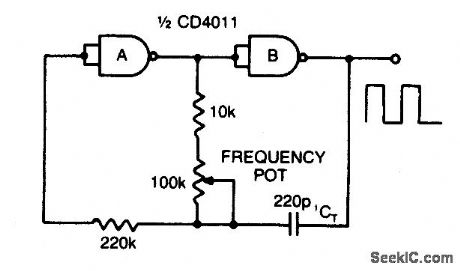
Varying the 100 K pot changes the discharge rate of CT and hence the frequency. A square wave output is generated. The maximum frequency using CMOS is limited to 2 MHz. (View)
View full Circuit Diagram | Comments | Reading(150)
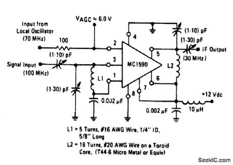
100_MHz_MIXER
Published:2009/6/25 21:34:00 Author:May
View full Circuit Diagram | Comments | Reading(2)
DOUBLY_BALANCEDMIXER(BROADBAND_INPUTS,90_MHz_TUNED_OUTPUT)
Published:2009/6/25 21:33:00 Author:May

View full Circuit Diagram | Comments | Reading(584)
20_dB_VIDEO
Published:2009/6/25 21:33:00 Author:May

Simple circuit having gain of 20 dB provides 3-dB bandwidth of 20 MHz for CA3100 bipolar MOS opamp. Total noise referred to input is only 35μV RMS.- Circuit Ideas for RCA Linear ICs, RCA Solid State Di-vision, Somerville, NJ, 1977, p 12. (View)
View full Circuit Diagram | Comments | Reading(619)
20_MHz_WIDEBAND
Published:2009/6/25 21:33:00 Author:May
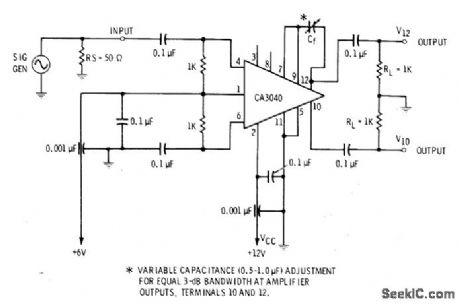
RCA CA3040 IC is connected for single-ended input and balanced output, with no resonant circuits. Gain is above 30 dB over wide frequency range.-E. M. Noll, Linear IC Principles, Experiments, and Proiects, Howard W. Sams, Indianapolis, IN, 1974, p 162-163 and 168. (View)
View full Circuit Diagram | Comments | Reading(956)
DIFFERENTIAL_PAIR
Published:2009/6/25 21:25:00 Author:May
Conventional differential amplifier circuit provides differential-mode gain of 96, common-mode input resistance of 500 megohms, CMRR of 106 dB, and current-source output resistance greater than 1 gigohm. Article gives design equations.-R. C. Jaeger and G. A.Hellwarth, Differential Cascade Amplifier Offers Unique Advantages, EDN Magazine, June 5, 1974, p 78 and 80. (View)
View full Circuit Diagram | Comments | Reading(1060)
ADJUSTABLE_TTL_CLOCK(MAINTAINS_50%DUTY_CYCLE)
Published:2009/6/25 21:25:00 Author:May

Symmetry of the square-wave output is maintained by connecting the right side of R2 through resistor R3 to the output of the third amplifier stage. This changes the charging cur-rent to the capacitors in proportion to the set-ting of frequency-adjusting potentiometer R2. Thus, a duty cycle of 50% is constant over the entire range of oscillation. The lower frequency limit is set by capacitor C2. With the components shown, the frequency of oscilla-tion can be varied by R2 from about 4 to 20 hertz. Other frequency ranges can be obtained by changing the values of C1 and R3, which control the upper limit of oscillation, or C2, which limits the low-frequency end. (View)
View full Circuit Diagram | Comments | Reading(787)
INVERSE_SCALER
Published:2009/6/25 21:25:00 Author:May
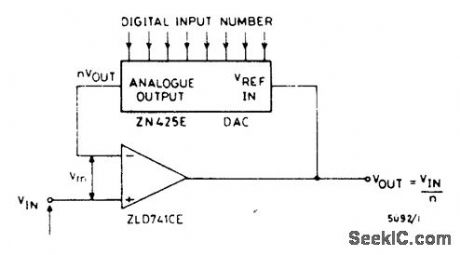
If a DAC is operated in the feedback loop of an operational amplifier,then the amplifiergain is inversely proportional to the input digital number or code to the DAC,The version giving scaling inversely proportional to posltive voltage is shown. (View)
View full Circuit Diagram | Comments | Reading(702)
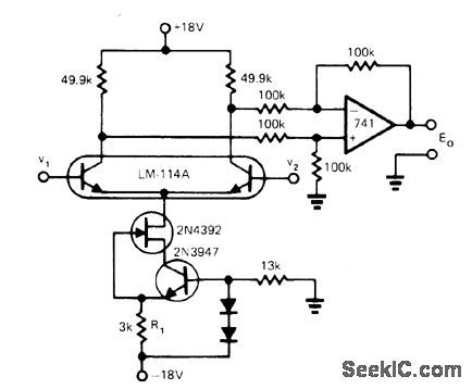
VOLTAGE_CONTROL_RESISTOR
Published:2009/6/25 21:24:00 Author:May
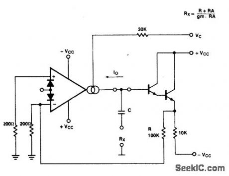
View full Circuit Diagram | Comments | Reading(716)
118_136_MHz_BROADBAND
Published:2009/6/25 21:24:00 Author:May
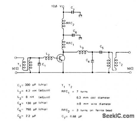
Designed for lowlevel amplitude modulation system. 50-ohm line transf ormers arewound with copperribbon on ferrite core to give 4:1 ratio. Design and con-struction procedures are covered. Transistor is Motorola 2N6083 rated 30 W for 4-W input.-B.Becciolini, Impedance Matching Networks Ap-plied to R-F Power Transistors, Motorola, Phoenix, AZ, 1974, AN-721, p 17. (View)
View full Circuit Diagram | Comments | Reading(1139)
SQUARE_WAVE_OSCILLATOR
Published:2009/6/25 21:24:00 Author:May
View full Circuit Diagram | Comments | Reading(0)
STEREO_BALANCE_METER
Published:2009/6/25 21:44:00 Author:Jessie
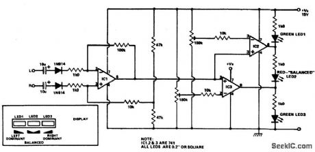
Outputs from each channel are fed to the two inputs of IC1 conrfected as a differential amplifier. IC2 and 3 are driven by the output of IC1. Output of IC1 is connected to the nonin-verting inputs of IC2 and 3. If the output of IC1 approaches the supply rail, the outputs of ICs 2 and 3 will also go high, illuminating LED3. This would happen if the right channel were dominating. If the left channel was dominant, the outputs of ICs 2 and 3 would be low, il-luminating LED1. If the two channels are equal in amplitude, the outputs of ICs 2 and 3 would be high and low respectively, lighting up LED2. (View)
View full Circuit Diagram | Comments | Reading(3136)
SQUAREWAVE_OSCILLATOR
Published:2009/6/25 21:43:00 Author:Jessie
View full Circuit Diagram | Comments | Reading(672)
SIMPLE_TRIANGLE_SQUARE_WAVE_OSCILLATOR
Published:2009/6/25 21:42:00 Author:Jessie
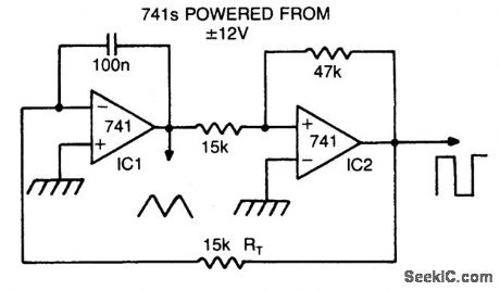
Circuit Notes By making Rr variable it IS possible to alter the operating frequency over a 100 to 1range,Versatile triangle/square wave oscillator has a possible frequency range of 0.1 Hz to 100 kHz. (View)
View full Circuit Diagram | Comments | Reading(6712)
05_Hz_SQUARE_WAVE_OSCILLATOR
Published:2009/6/25 21:41:00 Author:Jessie
View full Circuit Diagram | Comments | Reading(758)
| Pages:1298/2234 At 2012811282128312841285128612871288128912901291129212931294129512961297129812991300Under 20 |
Circuit Categories
power supply circuit
Amplifier Circuit
Basic Circuit
LED and Light Circuit
Sensor Circuit
Signal Processing
Electrical Equipment Circuit
Control Circuit
Remote Control Circuit
A/D-D/A Converter Circuit
Audio Circuit
Measuring and Test Circuit
Communication Circuit
Computer-Related Circuit
555 Circuit
Automotive Circuit
Repairing Circuit