
Circuit Diagram
Index 1299
MODULATION_MONITOR
Published:2009/6/25 21:41:00 Author:Jessie
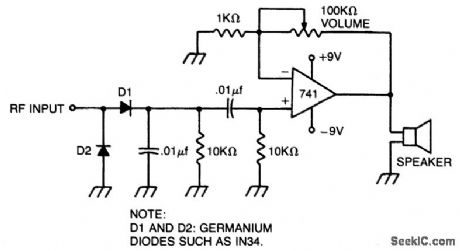
Broad-tuned recelver demodulates the RF signal picked up by a loosely coupled wire placed near the transmitting antenna. (View)
View full Circuit Diagram | Comments | Reading(1594)
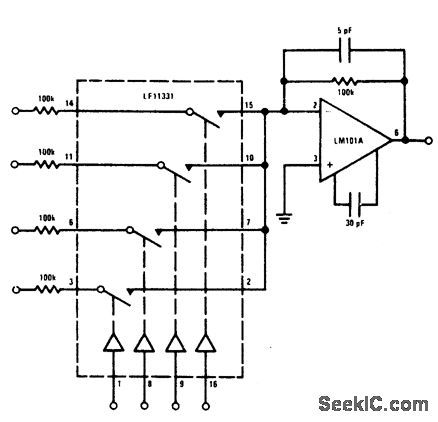
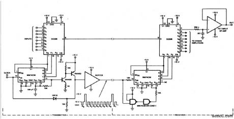
WIDE_BAND_DIFFERENTIAL_MULTIPLEXER
Published:2009/6/25 21:37:00 Author:Jessie
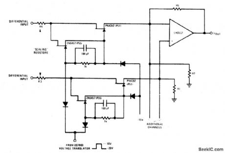
This design allows high frequency signal handling and high toggle rates simultane-ously.Toggie rates up to 1 MHz and MHz signals are possible with this circuit. (View)
View full Circuit Diagram | Comments | Reading(690)
NEGATIVE_PEAK_DETECTOR
Published:2009/6/25 21:36:00 Author:Jessie
View full Circuit Diagram | Comments | Reading(1692)
PRECISION_SQUARER
Published:2009/6/25 21:36:00 Author:Jessie
View full Circuit Diagram | Comments | Reading(0)
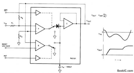
POSITIVE_PEAK_DETECTOR
Published:2009/6/25 21:36:00 Author:Jessie
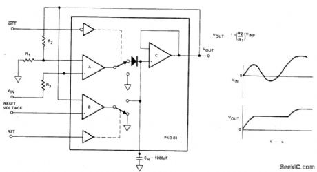
View full Circuit Diagram | Comments | Reading(3114)
MULTIPLEXER/MIXER_
Published:2009/6/25 21:35:00 Author:Jessie
View full Circuit Diagram | Comments | Reading(695)
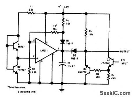
FREE_RUNNING_SQUARE_WAVE_OSCILLATOR
Published:2009/6/25 21:35:00 Author:Jessie
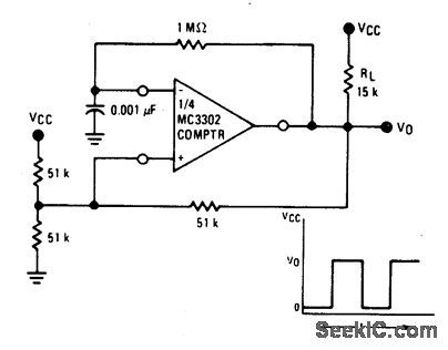
View full Circuit Diagram | Comments | Reading(670)
COMMON_SOURCE_MIXER
Published:2009/6/25 21:35:00 Author:Jessie
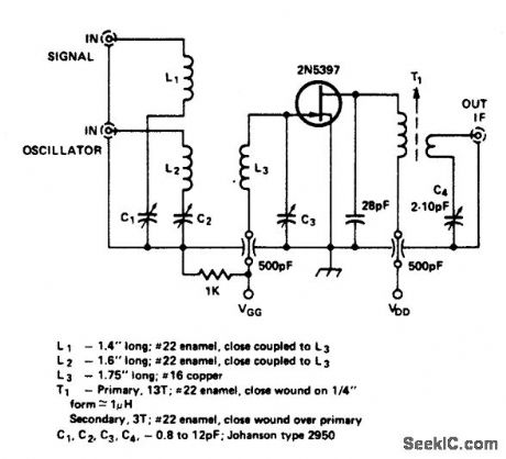
View full Circuit Diagram | Comments | Reading(655)
EIGHT_CHANNEL_MUX/DEMUX_SYSTEM
Published:2009/6/25 21:32:00 Author:Jessie
View full Circuit Diagram | Comments | Reading(651)
100_W_FOR_DC_TO_500_kHz
Published:2009/6/25 21:32:00 Author:Jessie
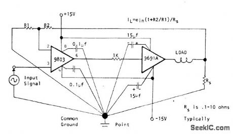
Circuit using Optical Electronics opamps has high input imped-ance, high gain capability, and 100-W output capacity without use of transformers, for highfidelity audio circuits, cathode-ray deflection circuits, and servosystems. Output currents up to 10 A require heavy output wiring, large power-supply bypass capacity, and heavy com-mon ground point. Load is in feedback loop of opamp. Constant-current drive for load makes impedance matching to loudspeaker unnecessary.- A High Gain 100 Watt Amplifier, Optical Electronics, Tucson, AZ, Application Tip 10205. (View)
View full Circuit Diagram | Comments | Reading(821)
1_kHz_SQUARE_WAVE_OSCILLATOR
Published:2009/6/25 21:22:00 Author:May
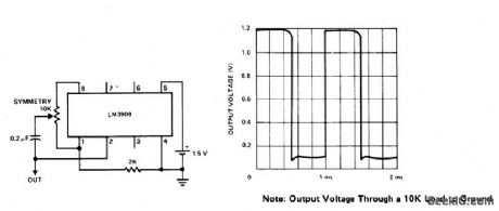
View full Circuit Diagram | Comments | Reading(0)
VOLTAGE_CONTROLLED_GAIN
Published:2009/6/25 21:32:00 Author:Jessie
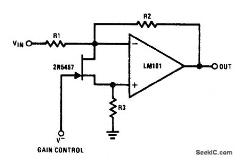
2N5457 FET acts as voltage-variable resistor between differential inputterminals of opamp. Resistance vat-iation is linear with voltage over several decades of resistance, to give excellent electronic gain control. Values of resistors depend on opamp used.- FET Databook, National Semi-conductor. Santa Clara, CA, 1977, p 6-26-6-36. (View)
View full Circuit Diagram | Comments | Reading(5784)
R_C_OSCILLATOR
Published:2009/6/25 21:21:00 Author:May
View full Circuit Diagram | Comments | Reading(0)
HIGH_INPUT_IMPEDANCE
Published:2009/6/25 21:31:00 Author:Jessie
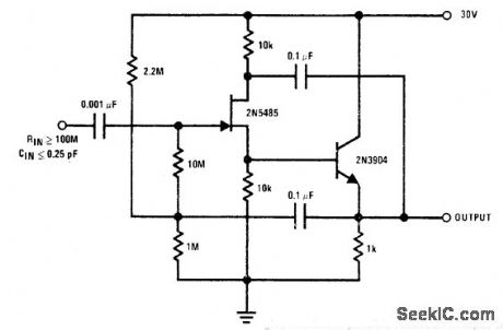
Simple JFET inputcircuit is operated as source follower with bootstrapped gate bias resistor and drain to give maximum possible reduction in input capacitance. Used as unity-gain AC amplifier.- FET Databook, National Semiconductor, Santa Clara, CA, 1977, p 6-26-6-36. (View)
View full Circuit Diagram | Comments | Reading(2)
TRIAC_TRIGGER
Published:2009/6/25 21:21:00 Author:May
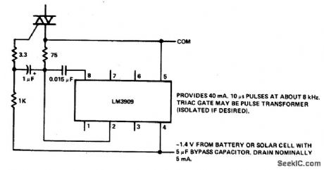
View full Circuit Diagram | Comments | Reading(0)
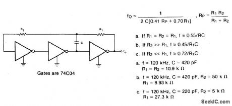
OSCILLATOR_CLOCK_GENERATOR_
Published:2009/6/25 21:31:00 Author:Jessie
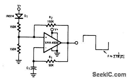
This self-starting fixed frequency oscillator circuit gives excellent frequency stability. R1 and C1 comprise the frequency determining network while R2 provides the regenerative feedback. Diode D1 enhances the stability by compensating for the difference between VOH and VSupply. In applications where a precision clock generator up to 100 kHz is required, such as in automatic test equipment, C1 may be replaced by a crystal. (View)
View full Circuit Diagram | Comments | Reading(605)
DIFFERENTIAL_MUX/DEMUX_SYSTEM
Published:2009/6/25 21:31:00 Author:Jessie
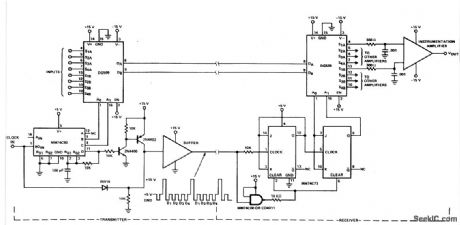
View full Circuit Diagram | Comments | Reading(672)
FOUR_CHANNEL_DATA_ACQUlSITION_SYSTEM
Published:2009/6/25 21:20:00 Author:May
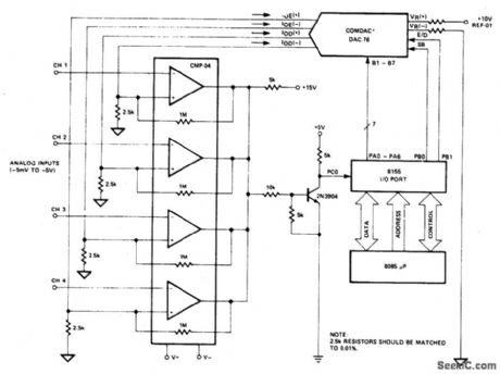
View full Circuit Diagram | Comments | Reading(0)
SOUND_OPERATED_TWO_WAY_SWITCH
Published:2009/6/25 21:20:00 Author:May
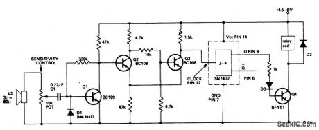
This circuit operates a relay each time a sound of sufficient intensity is made, thus one clap of the hands will switch it one way, a second clap will revert the circuit to the origi-nal condition. Q2 and Q3 form a Schmitt trigger. TheJK flip-flop is used as a bistable whose output changes state every time a pulse is applied to the clock input (pin 12). Q4 allows the output to drive a relay. (View)
View full Circuit Diagram | Comments | Reading(0)
PRODUCT_DETECTOR
Published:2009/6/25 21:29:00 Author:Jessie
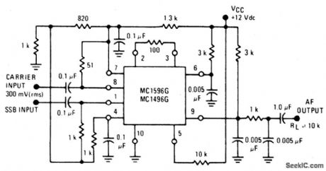
Circuit Notes
The MC1596/MC1496 makes an excellent SSB product detector. This product detec-tor has a sensitivity of 3.0 microvolts and a dynamic range of 90 dB when operating at an intermediate frequency of 9 MHz. The detector is broadband for the entire high frequency range. For operation at very low intermediate frequencies down to 50 kHz the 0.1μF capacitors on pins 7 and 8 should be increased to 1.0 μF. Also, the output filter at pin 9 can be tailored to a specific intermediate frequency and audio amplifier input impedange. The ernit-ter resistance between pins 2 and 3 may be increased or decreased to adjust circuit gain, sensitivity, and dynamic range. This circuit may also be used as an AM detector by intro-ducing carrier signal at the carrier input and an AM signal at the SSB input. The carrier signal may be derived from the intermediate fre-quency signal or generated cally. The carrier signal may be introduced with or without mod-ulation, provided its level is sufficiently high to saturate the upper quad differential amplifier. If the carrier signal is modulated, a 300 mV (rms) input level is recommended. (View)
View full Circuit Diagram | Comments | Reading(5)
| Pages:1299/2234 At 2012811282128312841285128612871288128912901291129212931294129512961297129812991300Under 20 |
Circuit Categories
power supply circuit
Amplifier Circuit
Basic Circuit
LED and Light Circuit
Sensor Circuit
Signal Processing
Electrical Equipment Circuit
Control Circuit
Remote Control Circuit
A/D-D/A Converter Circuit
Audio Circuit
Measuring and Test Circuit
Communication Circuit
Computer-Related Circuit
555 Circuit
Automotive Circuit
Repairing Circuit