
Circuit Diagram
Index 1287
BEAM_SPLITTER_FOR_OSCILLOSCOPE
Published:2009/6/26 2:27:00 Author:May
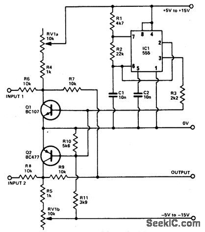
The basis of the beam splitter is a 555 timer connected as an astable multivibrator.Signals at the two inputs are alternately displayed on the oscilloscope with a clear separation between them. The output is controlled by the tandem potentiometer RV1a/b which also varies the amplitude of the traces. (View)
View full Circuit Diagram | Comments | Reading(862)
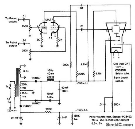
OSCILLOSCOPE_MONITOR
Published:2009/6/26 2:26:00 Author:May
View full Circuit Diagram | Comments | Reading(884)
FOUR_POSITION_MOTOR_SWITCH
Published:2009/6/26 2:25:00 Author:May
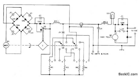
Single RF feed line also carries DC for 3-V permanent magnet DC motor B1 atop antenna tower, driving S3 and S4 for remote switching to antennas a, b, c, and d. Diagram shows switches set for feed to antenna a, with no drive applied to Bt since cam C has opened microswitch S5. CR5 and CR6 are now connected in series with opposite polarity, so neither positive nor negative halfwaves from 12-VAC supply can drive motor. If S2 is closed, poshive halfwaves start B1. Once started, motor runs until cam opens S5; if S2 has not yet been released, motor continues running on positive and negative halfwaves. Diode bridge CR1-CR4 makes motor rotate in only one direction for either drive polarity. If S2 is released, before S5 opens, motor stops. 6-V 1-A lamp DS1 comes on dimly when S2 is closed and brightens when S5 closes. If S2 is released now, B1 drives to next position and stops. If S2 is held down, switching continues. Meter M1 and CR7 identify position of switch. R1-R4 in range of 1K to 10K, are chosen to give 1/4, 1/2, 3/4, and full deflection of meter. Motor drives switch through 2860:1 reduction gears taken from alarm clock. All diodes are 50-PIV 1-A silicon such as 1N4001.-U.H.Lammers, A Remote Antenna Switch, QST,Aug.1974, p 41-43. (View)
View full Circuit Diagram | Comments | Reading(1043)
TRANSMITTER_OSCILLOSCOPE_COUPLER_FOR_CB_SIGNALS
Published:2009/6/26 2:24:00 Author:May
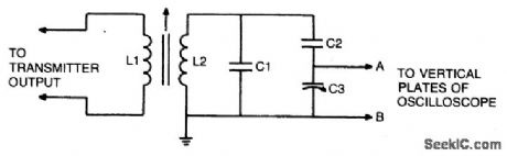
To display an rf signal, connect L1 to the transmitter and points A and B to the vertical plates of the oscilloscope. Adjust L1 for minimum SWR and C3 for the desired trace height on the CRT. L2 = 4 turns #18 on 3/4 slug tuned rf coil form, L1 = 3 turns #22 adjacent to grounded end of L1, C1, and C2 = 5 pF, C3 = 75 pF trimmer. (View)
View full Circuit Diagram | Comments | Reading(721)
DRAWING_CIRCLES_ON_ASCOPE
Published:2009/6/26 2:23:00 Author:May
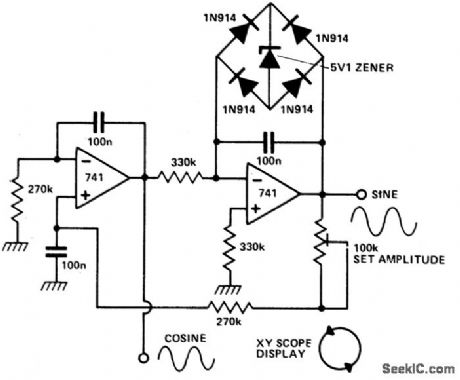
The circuit is that of a quadrature sine and cosine oscillator. To generate circular displays, connect the two outputs to the X and Y inputs. (View)
View full Circuit Diagram | Comments | Reading(884)
EARTH_CONDUCTMTY
Published:2009/6/26 2:23:00 Author:May
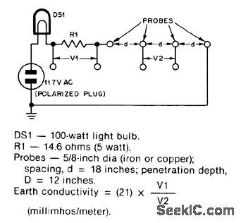
Simple AC measurement technique gives 25% accuracy, adequate for siting amateur radio antennas and designing radial ground systems. Measured values will range from 1 to 5 millimhos per meter for poor soil, 10-15 for average soil or flesh water,100 for very good soil, and 5000 for salt water.-J.Sevick, Short Grbund-Radial Systems for Short Verticals, QST,April 1978, p 30-33. (View)
View full Circuit Diagram | Comments | Reading(635)
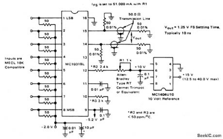
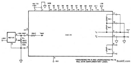
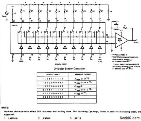
HIGH_SPEED_8_BIT_D_A_CONVERTER
Published:2009/6/26 2:23:00 Author:May
View full Circuit Diagram | Comments | Reading(966)
LINEAR_FIELD_STRENGTH_METER
Published:2009/6/26 2:22:00 Author:May
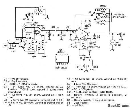
Has sufficient sensitivity for checking antenna patterns and gain while positioned many wavelengths from antenna. Can be used remotely by conlnecting external meter at J2. L1 is tuned by 01 for 80 or 40 meters. For 20, 15, or 10 meters, L2 is switched in parallel with L1. L5 and C2 coverabout 40 to 60 MHz, while L7 and C2 cover 130 to 180 MHz. Band-switched circuits avoid use of plug-in inductors. At most sensitive setting of S2, M1 will detect signals from pickup antenna as weak as 100μV.-L. McCoy, A Linear Field-Strength Meter, QST,Jan.1973,p18-20 and 35. (View)
View full Circuit Diagram | Comments | Reading(787)
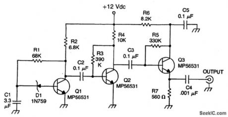
107_MHz_SWEEP_GENERATOR
Published:2009/6/26 2:22:00 Author:May
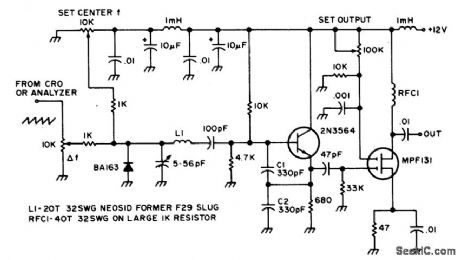
This circuit is used to observe the response of an if amp or a filter. It can be used with an oscilloscope or,for more dynamic range,with a spectrum analyzer. (View)
View full Circuit Diagram | Comments | Reading(1704)
8_BIT_D_A_CONVERTER
Published:2009/6/26 2:21:00 Author:May

View full Circuit Diagram | Comments | Reading(1306)
ADD_ON_TRIGGERED_SWEEP
Published:2009/6/26 2:20:00 Author:May
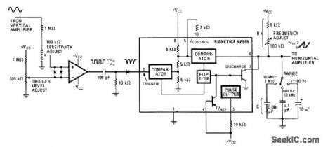
The circuit's input op amp triggers the timer, setting its flip-flop and cutting off its discharge transistor so that capacitor C can charge. When the capacitor voltage reaches the timer's control voltage (0.33Vcc), the flip-flop resets and the transistor conducts, discharging the capacitor. (View)
View full Circuit Diagram | Comments | Reading(774)
THREE_DIGIT_BCD_D_A_CONVERTER
Published:2009/6/26 2:17:00 Author:May
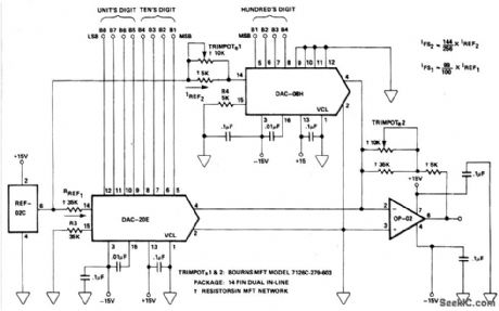
View full Circuit Diagram | Comments | Reading(890)
OSCILLOSCOPE_CONVERTER_PROVIDES_FOUR_CHANNEL_DISPLAYS
Published:2009/6/26 2:17:00 Author:May
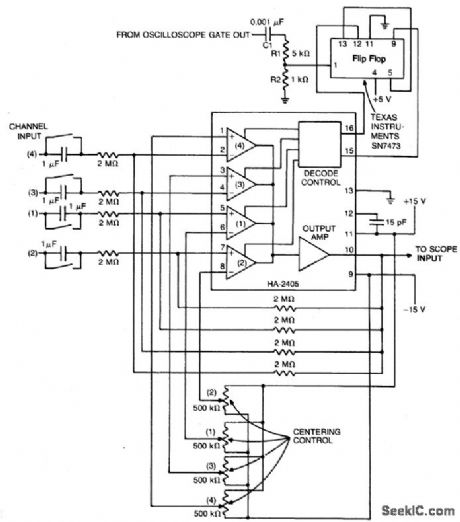
The monolithic quad operational amplifier provides an inexpensive way to increase display capability of a standard oscilloscope. Binary inputs drive the IC op amp; a dual flip-flop divides the scope's gate output to obtain channel selection signals. All channels have cen-tering controls for nulling offset voltage. AL negative-going scope gate signal selects the next channel after each trace. The circuit operates out to 5 MHz. (View)
View full Circuit Diagram | Comments | Reading(953)
RESISTOR_TERMINATED_DAC0_TO_5_V_OUTPUT
Published:2009/6/26 2:15:00 Author:May
View full Circuit Diagram | Comments | Reading(949)
NOISE_GENERATOR_CIRCUIT
Published:2009/6/26 2:15:00 Author:May
The zener diode is an avalanche rectifier in the reverse bias mode connected to the input circuit of a wideband rf amplifier. The noise is amplified and applied to the cascade wideband amplifier, transistors Q2 and Q3. (View)
View full Circuit Diagram | Comments | Reading(2163)
WIDEBAND_NOISE_GENERATOR
Published:2009/6/26 2:14:00 Author:May
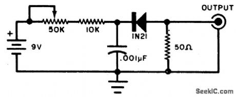
This circuit will produce wideband rf noise. It uses a reverse-biased diode and has a low-impedance output. Can be used to align receivers for optimum performance. (View)
View full Circuit Diagram | Comments | Reading(3463)
NOISE_GENERATOR
Published:2009/6/26 2:13:00 Author:May
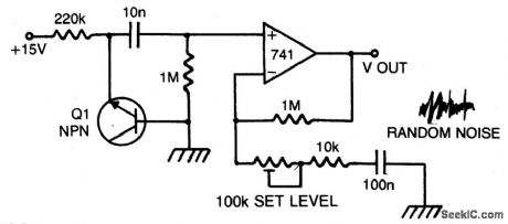
The zener breakdown of a transistor junction is used as a noise generator. The breakdown mechanism is random and this voltage has a high source impedance. By using the op amp as a high input impedance, high ac gain amplifier, a low impedance, large signal noise source is obtained. The 100K potentiometer is used to set the noise level by varying the gain from 40 to 20 dB. (View)
View full Circuit Diagram | Comments | Reading(0)
PINK_NOISE_GENERATOR
Published:2009/6/26 2:12:00 Author:May
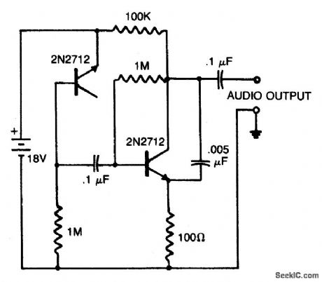
A reverse-biased pn junction of a 2N2712 transistor is used as a noise generator. The second 2N2712 is an audio amplifier. The 0.005 μF capacitor across the amplifier output remove s some high-frequency components to simulate pink noise more closely. The audio output may be connected to high-impedance earphones or to a driver amplifier for speaker listening. (View)
View full Circuit Diagram | Comments | Reading(0)
FAST_VOLTAGE_OUTPUT_D_A_CONVERTER
Published:2009/6/26 2:11:00 Author:May
View full Circuit Diagram | Comments | Reading(797)
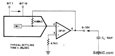
10_BIT_D_A_CONVERTER
Published:2009/6/26 2:10:00 Author:May
0p-Amp characteisties effect D/A accuracy and setding time. The following Op-Amps, listed in order of increasing speed, are suggested:1.LM101A 2.LF156A 3.LM118 (View)
View full Circuit Diagram | Comments | Reading(978)
| Pages:1287/2234 At 2012811282128312841285128612871288128912901291129212931294129512961297129812991300Under 20 |
Circuit Categories
power supply circuit
Amplifier Circuit
Basic Circuit
LED and Light Circuit
Sensor Circuit
Signal Processing
Electrical Equipment Circuit
Control Circuit
Remote Control Circuit
A/D-D/A Converter Circuit
Audio Circuit
Measuring and Test Circuit
Communication Circuit
Computer-Related Circuit
555 Circuit
Automotive Circuit
Repairing Circuit