
Circuit Diagram
Index 1288
AUDIO_NOISE_GENERATOR
Published:2009/6/26 2:10:00 Author:May

This simple circuit generates both white and pin noise. Transistor Q1 is used as a zener diode. The normal base-emitter junction is reverse-biased and goes into zener breakdown at about 7 to 8 volts. The zener noise current from Q1 floirs into the base of Q2 such that an output of about 150 millivolts of white noise is available. To convert the white noise to pink, a filter is required which provides a 3 dB cut per octave as the frequency increases.Since such a filter attenuates the noise considerably an amplifier is used to restore the output level. Transistor Q3 is this amplifier and the pink noise filter is connected as a feedback network. between collector and base in order to obtain the required characteristic by controlling the gain-yersus-fre quency of the transistor. The output of transistor Q3 is thus the pink noise required and is fed to the relevant output socket. (View)
View full Circuit Diagram | Comments | Reading(3016)
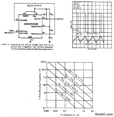
100_kHz_FREE_RUNNING_MULTIVIBRATOR
Published:2009/6/26 2:08:00 Author:May
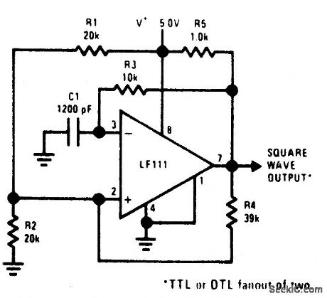
View full Circuit Diagram | Comments | Reading(726)
MONOSTABLE_MULTIVIBRATOR
Published:2009/6/26 2:08:00 Author:May
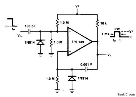
View full Circuit Diagram | Comments | Reading(0)
BISTABLE_MULTIVIBRATOR
Published:2009/6/26 2:07:00 Author:May
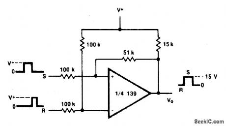
View full Circuit Diagram | Comments | Reading(0)
ONE_SHOT_MULTIVIBRATOR_
Published:2009/6/26 2:07:00 Author:May
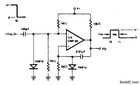
View full Circuit Diagram | Comments | Reading(910)
1MONOSTABLE_CIRCUIT
Published:2009/6/26 2:04:00 Author:May
View full Circuit Diagram | Comments | Reading(639)
TTL_MONOSTABLE
Published:2009/6/26 2:04:00 Author:May

View full Circuit Diagram | Comments | Reading(1384)
MONOSTABLE_MULTIVIBRATOR_WITH_INPUT_LOCK_OUT
Published:2009/6/26 2:03:00 Author:May
View full Circuit Diagram | Comments | Reading(697)
UJT_MONOSTABLE
Published:2009/6/26 2:02:00 Author:May
View full Circuit Diagram | Comments | Reading(650)
14_BIT_BINARY_D_A_CONVERTERUNIPOLAR
Published:2009/6/26 2:02:00 Author:May
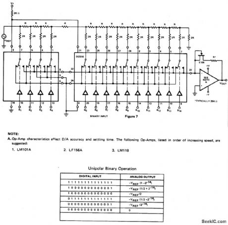
View full Circuit Diagram | Comments | Reading(780)
DUAL_ASTABLE_MULTIVIBRATOR
Published:2009/6/26 2:02:00 Author:May
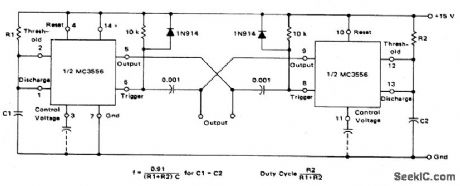
This dual astable multivibrator provides versatility not available with single timer circuits. The duty cycle can be adjusted from 5% to 95%. The two outputs provide two phase clock signals often required in digital systems.It can also be inhibited by use of either reset terminal. (View)
View full Circuit Diagram | Comments | Reading(726)
DIGITALLY_CONTROLLED_ASTABLE_M_ULTIVIBRATOR
Published:2009/6/26 2:00:00 Author:May
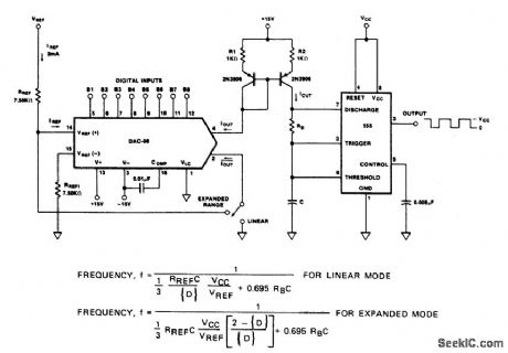
View full Circuit Diagram | Comments | Reading(534)
ASTABLE_OSCILLATOR
Published:2009/6/26 1:59:00 Author:May
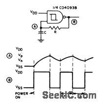
Before power is applied, the input and output are at ground potential and capacitor C is discharged. On power-on, the output goes high (VDD) and C charges through R until Vis reached. the output then goes low (VSS). C is now discharged through R until Vn is reached.The output then goes high and charges C towards Vp through R. Thus input A alternately swings between Vp and Vn as the output goes high and low. This circuit is self-starting at power-on. (View)
View full Circuit Diagram | Comments | Reading(913)
WINDOW_DETECTOR_
Published:2009/6/26 1:57:00 Author:May
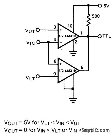
View full Circuit Diagram | Comments | Reading(780)
ASTABLE_MULTIVIBRATOR
Published:2009/6/26 1:56:00 Author:May
The capacitor C will charge through RA and RB, and then discharge through RB only.The duty cycle may be controlled by the values of RA and RB. (View)
View full Circuit Diagram | Comments | Reading(0)
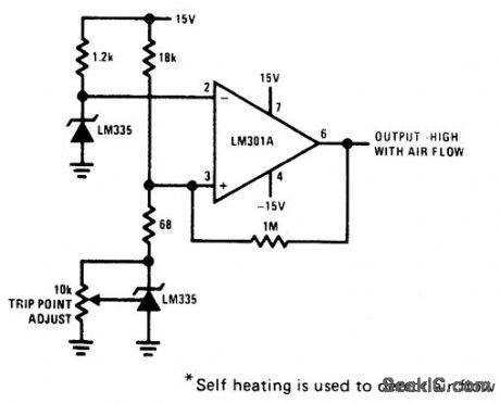
AIR_FLOW_DETECTOR__
Published:2009/6/26 1:56:00 Author:May
View full Circuit Diagram | Comments | Reading(646)
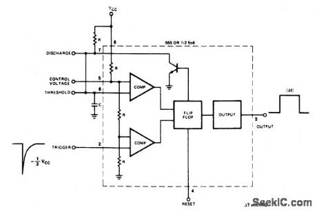
MONOSTABLE_CIRCUIT
Published:2009/6/26 1:54:00 Author:May
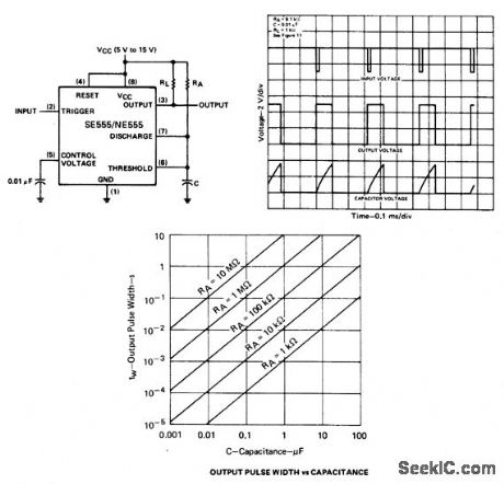
If the output is low, application of a negative-going pulse to the trigger input sets the flip-flop (Q goes low), drives the output high, and turns off 1. Capacitor C is then charged through Ra until the voltage across the capacitor reaches the threshold voltage of the threshold input. If the trigger input has returned to a high level, the output of the threshold comparator will reset the flip-flop (Q goes high), drive the output low, and discharge C through Q1. Monostable operations is initiated when the trigger input voltage falls below the trigger threshold. Once initiated, the sequence will complete only if the trigger input is high at the end of the timing interval. (View)
View full Circuit Diagram | Comments | Reading(846)
AC_SERVO_AMPLIFIER_BRIDGE_TYPE
Published:2009/6/26 1:52:00 Author:May
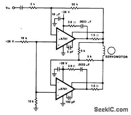
View full Circuit Diagram | Comments | Reading(624)
POWER_TOOL_TORQUE_CONTROL
Published:2009/6/26 1:51:00 Author:May
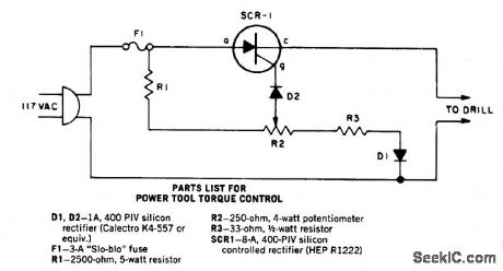
As the speed of an electric drill is decreased by loading, its torque also drops. A compensating speed control like this one puts the oomph back into the motor. When the drill slows down, a back voltage developed across the motor-in series with the SCR cathode and gate-decreases. The SCR gate voltage therefore increases relatively as the back voltage is reduced. The extra gate voltage causes the SCR to conduct over a larger angle and more current is driven into the drill, even as speed falls under load. The SCR should be mounted in 1/4-in. thick block of aluminum or copper at least 1-in. square. If the circuit is used for extended periods use a 2 inch square piece. (View)
View full Circuit Diagram | Comments | Reading(3549)
DC_SERVO_AMPLIFIER
Published:2009/6/26 1:50:00 Author:May
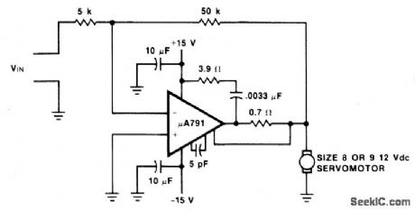
View full Circuit Diagram | Comments | Reading(760)
| Pages:1288/2234 At 2012811282128312841285128612871288128912901291129212931294129512961297129812991300Under 20 |
Circuit Categories
power supply circuit
Amplifier Circuit
Basic Circuit
LED and Light Circuit
Sensor Circuit
Signal Processing
Electrical Equipment Circuit
Control Circuit
Remote Control Circuit
A/D-D/A Converter Circuit
Audio Circuit
Measuring and Test Circuit
Communication Circuit
Computer-Related Circuit
555 Circuit
Automotive Circuit
Repairing Circuit