
Circuit Diagram
Index 1297
1TV_MODULATOR
Published:2009/6/25 21:56:00 Author:May
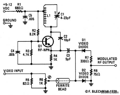
The VHF frequency is generated by a tuned Hartley oscillator circuit. Resistors R2, R3, and R4 bias the transistor, with tapped inductor L1 and trimmercapacitor C1 forming the tank circuit. Adjusting C1 determines the frequdncy. Capacitor C2 provides positive feedback from the tank circuit to the emitter at Q1. Capacitor C4 provides an RF ground for the base of Q1. Bypass capacitor C5 and resistor R1 filter out the radio frequencies generated in the tank circuit to prevent radiation from the power-supply lines. The video signal enters the parallel combination of resistors R5 and R6; this combination closely matches the 75 ohm impedance of most video cables. Resistor R6 is a small screwdrtver-adjusted potentiometer that is used to control the video input level to mixer diodes D1 and D2. (View)
View full Circuit Diagram | Comments | Reading(1310)
TWO_CHANNEL_SWITCH
Published:2009/6/25 21:56:00 Author:May
View full Circuit Diagram | Comments | Reading(724)
TV_MODULATOR
Published:2009/6/25 21:53:00 Author:May
The FM oscillator/modulator is a voltage-controlled oscillator, which exhibits a nearly linear output frequency versus input voltage characteristic for a wide deviation. It provides a good FM source with a few inexpensive external parts. It has a frequency range of 1.4 to 14 MHz and can typically produce a ±25 kHz modulated 4.5 MHz signal with about 0.6% total harmonic distortion. (View)
View full Circuit Diagram | Comments | Reading(0)
HIGH_FREQUENCY_SWITCH
Published:2009/6/25 21:53:00 Author:May

The 2N4391 provides a low ON resistance of 30 ohm and a high OFF impedance (<0.2 pF) when off. With proper layout and an ideal switch, the performance stated above can be readily achieved. (View)
View full Circuit Diagram | Comments | Reading(0)
DIFFERENTIAL_ANALOG_SWITCH
Published:2009/6/25 21:52:00 Author:May
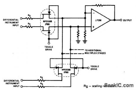
The NPD5566 monolithic dual is used in a differential multiplex application where Rd,coN) should be closely matched. Since Rd,coN) for the monolithic dual tracks at better than ±1% over wide temperature ranges (- 25℃ to +125℃), this makes it an unusual but ideal choice for an accurate multiplexer. This close tracking greatly reduces errors due to common-mode signals. (View)
View full Circuit Diagram | Comments | Reading(0)
TRIAC_ZERO_VOLTAGE_SWITCHING
Published:2009/6/25 21:55:00 Author:Jessie
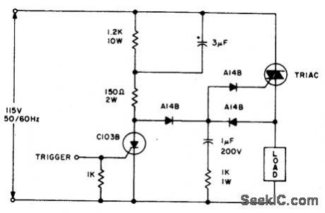
The triac will be gated on at the start of the positive half cycle by current flow through the 3 μF capacitor as long as the C103 SCR is off. The load voltage then charges up the 1 μF capacitor so that the triac will again be ener-gized during the subsequent negative half cycle of line voltage. A selected gate triac is required because of the triggering mode. (View)
View full Circuit Diagram | Comments | Reading(1728)
TV_MODULATOR
Published:2009/6/25 21:53:00 Author:Jessie
The FM oscillator/modulator is a voltage-controlled oscillator, which exhibits a nearly linear output frequency versus input voltage characteristic for a wide deviation. It provides a good FM source with a few inexpensive external parts. It has a frequency range of 1.4 to 14 MHz and can typically produce a ±25 kHz modulated 4.5 MHz signal with about 0.6% total harmonic distortion. (View)
View full Circuit Diagram | Comments | Reading(1906)
HIGH_FREQUENCY_SWITCH
Published:2009/6/25 21:53:00 Author:Jessie
The 2N4391 provides a low ON resistance of 30 ohm and a high OFF impedance (<0.2 pF) when off. With proper layout and an ideal switch, the performance stated above can be readily achieved. (View)
View full Circuit Diagram | Comments | Reading(1400)
DIFFERENTIAL_ANALOG_SWITCH
Published:2009/6/25 21:52:00 Author:Jessie
The NPD5566 monolithic dual is used in a differential multiplex application where Rd,coN) should be closely matched. Since Rd,coN) for the monolithic dual tracks at better than ±1% over wide temperature ranges (- 25℃ to +125℃), this makes it an unusual but ideal choice for an accurate multiplexer. This close tracking greatly reduces errors due to common-mode signals. (View)
View full Circuit Diagram | Comments | Reading(1823)
HIGH_TOGGLE_RATE_HIGH_FREQUENCY_ANALOG_SWITCH
Published:2009/6/25 21:49:00 Author:May
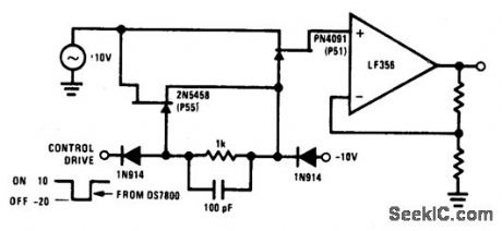
Commutator circuit provides low tmpedance gate drive to the PN4091 analog switch for both on and offdrive conditions.This circuit also approaches the ideal gate drive conditions for high frequency signal handling by providing a low ac impedance for off drive and high ac impedance for on drive to the PN4091 (View)
View full Circuit Diagram | Comments | Reading(0)
VIDEO_ATTENUATOR
Published:2009/6/25 21:52:00 Author:Jessie
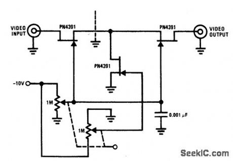
FETs in T attenuator provide optimum dynamic linear range for at-tenuation of video signals with ganged 1-meg-ohm pots. If complete turnoff is desired, atten-uatlon greater than 100 dB can be obtained at 10 MHz by using appropriate RF construction to minimize leakage. ON resistance of transistor (between drain and source) is less than 30 ohms.- FET Databook, National Semicon-ductor, Santa Clara, CA, 1977, p 6-26-6-36. (View)
View full Circuit Diagram | Comments | Reading(742)
50_MHz_POWER
Published:2009/6/25 21:49:00 Author:May
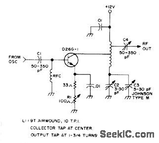
Developed for use with 50 MHz microtransistor crystal oscillator,using additional GE microtransistor for boosting RF output to about 75 mW,Article covers construction with microcomponents and gives other microtransistor circuits for low-power amateur tadiouse and possible bugging applications,-B.Hoisington、Introduction to″Microtransistors,″73 Magazit, Oct.1974,p 24-30. (View)
View full Circuit Diagram | Comments | Reading(1580)
DTL_TTL_CONTROLLED_BUFFERED_ANALOG_SWITCH
Published:2009/6/25 21:48:00 Author:May
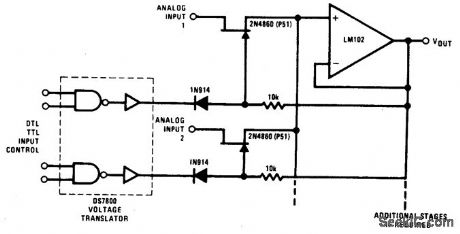
This analog switch uses the 2N4860 JFET for its 25 ohm ron and low leakage. The LM102 serves as a voltage buffer. This circuit can be adapted to a dual trace oscilloscope chopper. The DS7800 monolithic IC provides adequate switch drive controlled by DTL/TTL logic levels. (View)
View full Circuit Diagram | Comments | Reading(0)
PREAMP_F0R_O5_Hz_T0_2_MHz
Published:2009/6/25 21:50:00 Author:Jessie
Provides 11-dB gain over entire frequency range, with input impedance of 32 megohms. Q3 is GE-2 or HEP-52, and other transistors are SK3020 or HEP-53.-Circuits, 73Magazine, Jan. 1974, p 125. (View)
View full Circuit Diagram | Comments | Reading(785)
20_dB_VIDEO_LINE_DRIVER
Published:2009/6/25 21:50:00 Author:Jessie
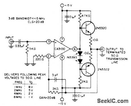
RCA CA3100 wideband opamp and power transistor output stage together provide gain of 20 dB at video frequencies for driving 50-ohm line. Peak output voltage ranges from 8V at 1MHz to 1V at 8MHz Upper frequency limit for unity galn is about 38MHz.- Linear Integrated Circuits and MOS/FET's、″RCA Solid State Division,Somerville,NJ,1977,p 225-227 (View)
View full Circuit Diagram | Comments | Reading(1423)
CB_MODULATION_MONITOR
Published:2009/6/25 21:48:00 Author:May
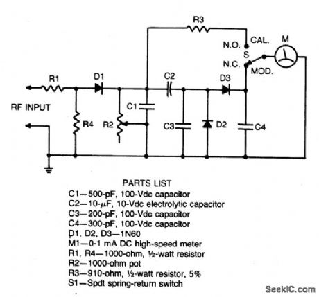
Connect this circuit to a transceiver with a coaxial T connector in the transmission line. Key the transmitter (unmodulated), set S1 to CAL, and adjust R2 for a full scale reading. Return S1 to MOD position. The meter will read % modulation with 10% accuracy. (View)
View full Circuit Diagram | Comments | Reading(0)
HIGH_TOGGLE_RATE_HIGH_FREQUENCY_ANALOG_SWITCH
Published:2009/6/25 21:49:00 Author:Jessie
Commutator circuit provides low tmpedance gate drive to the PN4091 analog switch for both on and offdrive conditions.This circuit also approaches the ideal gate drive conditions for high frequency signal handling by providing a low ac impedance for off drive and high ac impedance for on drive to the PN4091 (View)
View full Circuit Diagram | Comments | Reading(1266)
STEREO_BALANCE_METER_1
Published:2009/6/25 21:47:00 Author:May
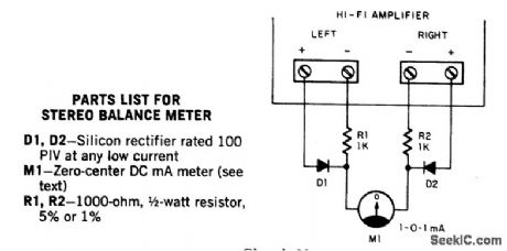
Play any stereo disc or tape and then set the amplifier to mono. Adjust left and right channel balance until meter M1 indicates zero; then the left and right output level are identical. (View)
View full Circuit Diagram | Comments | Reading(678)
50_MHz_POWER
Published:2009/6/25 21:49:00 Author:Jessie
Developed for use with 50 MHz microtransistor crystal oscillator,using additional GE microtransistor for boosting RF output to about 75 mW,Article covers construction with microcomponents and gives other microtransistor circuits for low-power amateur tadiouse and possible bugging applications,-B.Hoisington、Introduction to″Microtransistors,″73 Magazit, Oct.1974,p 24-30. (View)
View full Circuit Diagram | Comments | Reading(0)
DTL_TTL_CONTROLLED_BUFFERED_ANALOG_SWITCH
Published:2009/6/25 21:48:00 Author:Jessie
This analog switch uses the 2N4860 JFET for its 25 ohm ron and low leakage. The LM102 serves as a voltage buffer. This circuit can be adapted to a dual trace oscilloscope chopper. The DS7800 monolithic IC provides adequate switch drive controlled by DTL/TTL logic levels. (View)
View full Circuit Diagram | Comments | Reading(1282)
| Pages:1297/2234 At 2012811282128312841285128612871288128912901291129212931294129512961297129812991300Under 20 |
Circuit Categories
power supply circuit
Amplifier Circuit
Basic Circuit
LED and Light Circuit
Sensor Circuit
Signal Processing
Electrical Equipment Circuit
Control Circuit
Remote Control Circuit
A/D-D/A Converter Circuit
Audio Circuit
Measuring and Test Circuit
Communication Circuit
Computer-Related Circuit
555 Circuit
Automotive Circuit
Repairing Circuit