
Circuit Diagram
Index 1296
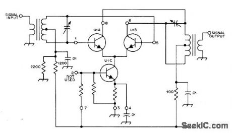
MODULATOR_
Published:2009/6/25 22:09:00 Author:May
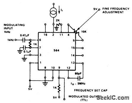
View full Circuit Diagram | Comments | Reading(741)
BALANCED_MODULATOR_(+12_Vdc_SINGLE_SUPPLY)
Published:2009/6/25 22:09:00 Author:May
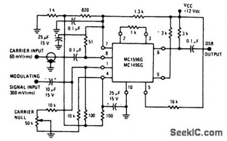
View full Circuit Diagram | Comments | Reading(619)
50_dB_BROADBAND_VIDEO
Published:2009/6/25 22:08:00 Author:May
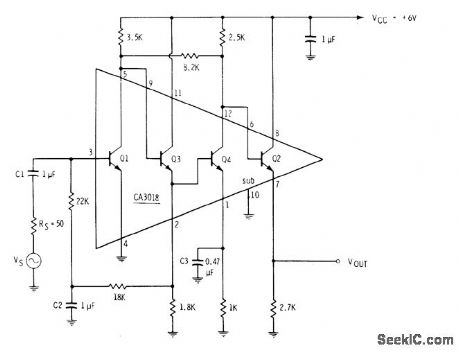
RCA CA3018 fourtransistor array is connected as two pairs of common-emitter emitter-follower combinations, with two feedback loops providing high DC stabilhy. One path goes from emitter of Q3 back to input, and other goes from collector of Q4 to collector of Q1. Values of C1, C2, and C3 give low-frequency cutoff (3 dB down) of 800 Hz.Upper cutoff is 32 MHz.-E.M.Noll, Linear IC Principles, Experiments, and Projects, Howard W. Sams, Indianapolis, IN,1974, p 165-168 and 174.
(View)
View full Circuit Diagram | Comments | Reading(742)
VIDEO_MODULATOR_
Published:2009/6/25 22:07:00 Author:May

View full Circuit Diagram | Comments | Reading(1571)
LINEAR_PULSE_WIDTH_MODULATOR
Published:2009/6/25 22:07:00 Author:May
View full Circuit Diagram | Comments | Reading(777)
TELEPHONE_LINE_MONITOR
Published:2009/6/25 22:06:00 Author:May
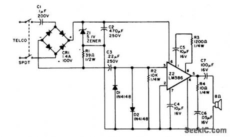
Using rectified audio as a power supply, this monitor will send the telephone line audio into an 8 ohm speaker. (View)
View full Circuit Diagram | Comments | Reading(132)
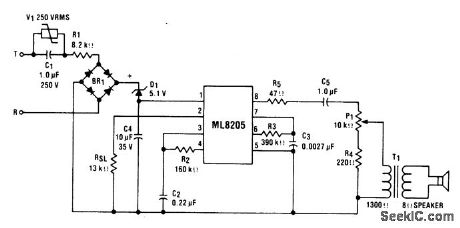
TELEPHONE_OR_EXTENSION_TONE_RINGER
Published:2009/6/25 22:06:00 Author:May
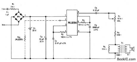
This circuit uses ML8204/ML8205 devices. With the components shown, theoutput frequency chops between 512 Hz (fH1) and 640 Hz (fH2) at a10 Hz (fL) rate. (View)
View full Circuit Diagram | Comments | Reading(1998)
RE_MODULATOR
Published:2009/6/25 22:05:00 Author:May
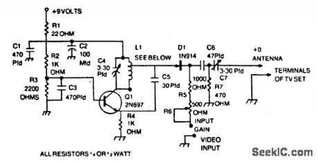
Capacitors C1, C3, C5, and C6 should be dipped mica. C4 and C7 are compression or piston trimmer types. R6 is PC-board mount trimpot. L1 is 6 tums of No.14 enameled wire, 3/8 inch I.D. by 3/4 inch long, tapped at 1 turn from top. (View)
View full Circuit Diagram | Comments | Reading(776)
HIGH_IMPEDANCE_VlDEO
Published:2009/6/25 22:04:00 Author:May
Compound seriesfeedback circuit using FET at input provides high input impedance and stable wideband gain for general-purpose video amplifier applica-tions.- FET Databook, National Semicon-ductor, Santa Clara, CA 1971, p 6-26-6-36. (View)
View full Circuit Diagram | Comments | Reading(804)
RF_DIFFERENTIAL_AMPLIFIER
Published:2009/6/25 22:04:00 Author:May
Uses RCAC CA3028A linear IC to provide power gain ofabout 32 dB at frequencies up to about 120MHz,Values of tuned circuits deρend on frequency used Unmarked resistors are on IC -D.DeMaw、Vndelstanding Linear ICs、QST, Feb1977、p19 (View)
View full Circuit Diagram | Comments | Reading(794)
STABILIZED_BIAS
Published:2009/6/25 22:03:00 Author:May
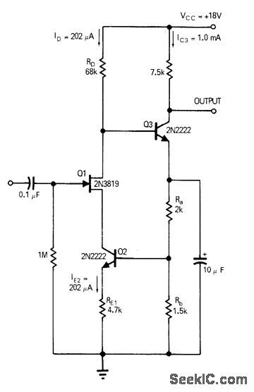
Simple voltage-feedback loop stabilizes bias on direct-coupled FET and bipolar transistor stages. Arrangement uses constant-current source a2 to maintain stable bias voltage on base of 03. By choosing proper resistor values, DC voltage feedback from emitter of bipolar is made to control constant-cur-rent value. Any change in drain current pro-duces opposite change in constant-current value, for stabilizing bipolar. Article gives de-sign equation.-H. T. Russell, DC Feedback Stabilizes Bias on FETTBipolar Pair, EDN Magazine, Nov.15,1970, p 51. (View)
View full Circuit Diagram | Comments | Reading(1158)
FCC_APPROVED_TELEPHONE_TONE_RINGER
Published:2009/6/25 22:03:00 Author:May
View full Circuit Diagram | Comments | Reading(1234)
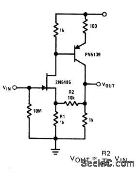
POLARITY_IGNORlNG_VOLTAGE_FOLLOWER
Published:2009/6/25 22:02:00 Author:May
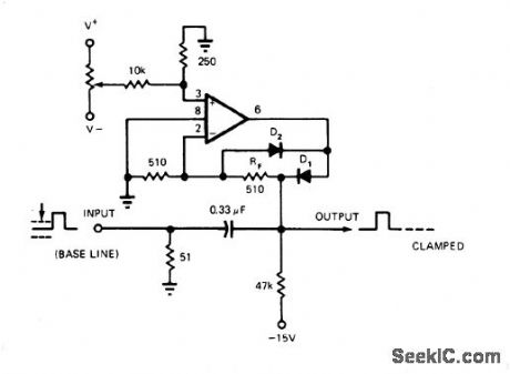
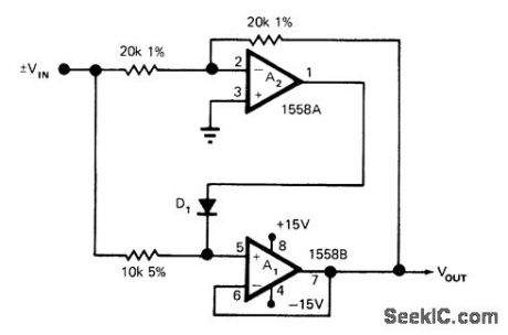
Absolute-value circuit is basically voltage follower A1 whose input is positive regardless of polarity of VIN. With positive input, inverting amplifier A2 is disconnected by D1. With negative input, inverting amplifier applies poshive input to voltage follower through D1. Output voltage is thus absolute value of input voltage.-R. J. Wincentsen, Absolute Value Circuit Uses Only Five Parts, EDN Magazine, Nov. 1,1972, p 44. (View)
View full Circuit Diagram | Comments | Reading(1665)
TELEPHONE_TONE_RINGER
Published:2009/6/25 22:02:00 Author:May
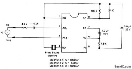
This is a complete telephone bell replacement circuit with minimum external components with on-chip diode bridge and transient protection and direct drive for piezoelectric transducers. (View)
View full Circuit Diagram | Comments | Reading(892)
1PULSE_WIDTH_MODULATOR
Published:2009/6/25 22:02:00 Author:May
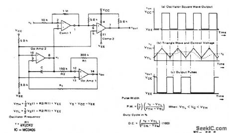
View full Circuit Diagram | Comments | Reading(746)
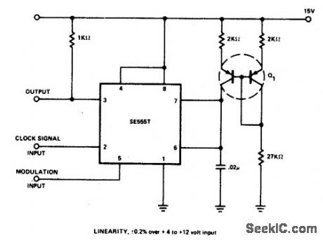
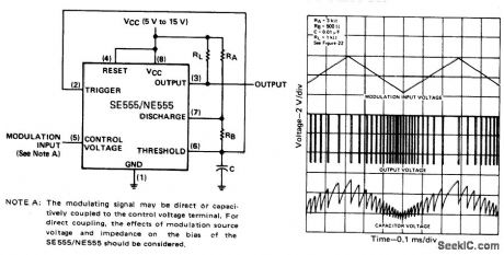
PULSE_WIDTH_MODULATOR
Published:2009/6/25 22:00:00 Author:May
If the timer is triggered with a continuous pulse train in the monostabie mode of operation, the charge time of the capacitor can be varied by changing the control voltage at pin 3.In this manner, the output pulse width can be modulated by applying a modulating signal that controls the threshold voltage. (View)
View full Circuit Diagram | Comments | Reading(0)
TELEPHONE_STATUS_MONITOR_USING_AN_oPTOISOLATOR
Published:2009/6/25 22:00:00 Author:May
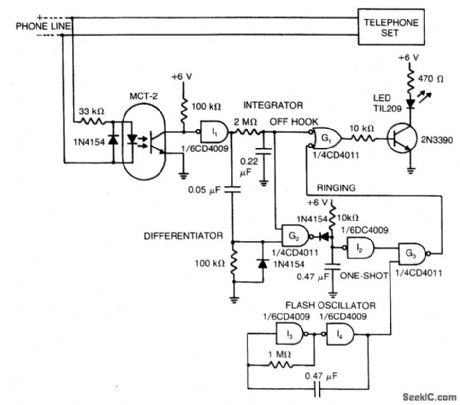
The LED indicates the status of a remote telephone. The light is off if the phone is hung up. It shines steadily if the phone is off hook, and it flashes on and off while phone rings and for 5 seconds after ringing stops. The flashing oscillator operates continuously but can drive the LED only when a ringing signal discharges the one shot capacitor to enable NAND gate G3. Thus, one oscillator handles several phone lines. (View)
View full Circuit Diagram | Comments | Reading(835)
PORTABLE_TONE_GENERATOR
Published:2009/6/25 21:58:00 Author:May
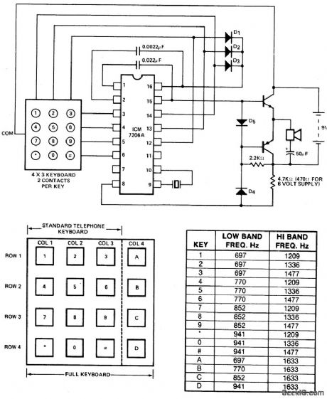
View full Circuit Diagram | Comments | Reading(653)
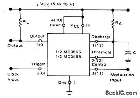
PULSE_POSITION_MODULATOR
Published:2009/6/25 21:58:00 Author:May
The threshold voltage, and thereby the time delay, of a free-running oscillator is shown modulated with a triangular-wave modulation signal; however, any modulating wave-shape could be used. (View)
View full Circuit Diagram | Comments | Reading(2)
10_A_25_Vdc_SOLID_STATE_RELAYS
Published:2009/6/25 21:57:00 Author:May
View full Circuit Diagram | Comments | Reading(699)
| Pages:1296/2234 At 2012811282128312841285128612871288128912901291129212931294129512961297129812991300Under 20 |
Circuit Categories
power supply circuit
Amplifier Circuit
Basic Circuit
LED and Light Circuit
Sensor Circuit
Signal Processing
Electrical Equipment Circuit
Control Circuit
Remote Control Circuit
A/D-D/A Converter Circuit
Audio Circuit
Measuring and Test Circuit
Communication Circuit
Computer-Related Circuit
555 Circuit
Automotive Circuit
Repairing Circuit