
Circuit Diagram
Index 1301
1_36_MHz_DISTRIBUTED
Published:2009/6/25 21:23:00 Author:Jessie
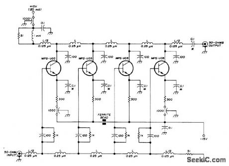
ProvkIes 18-dB gain over entire frequency range without use of special ferrite transformers, Gain contribution of each transistor, in phase with amplified wave as it passes down artificial transmission line, adds to that of other transistors. Capacitors marked with asterisks are lowinductance ceramic types such as Efie Redcap. Delay-line inductors L are 12 turns No.24 closewound on 1/8-inch diameter Lucite rod, and L/2 units are 7 turns. Can be used as preamp for frequency counter and as auxiliary for other test equipment. Article covers construction, heatsinking of transistor, and testing.-H. Olson, WidRange Broadband Amplifier, Ham Radio, April 1974, p 40-44. (View)
View full Circuit Diagram | Comments | Reading(1237)
TTL_OSCILLATOR
Published:2009/6/25 21:23:00 Author:Jessie

TTL inverter stages, U1 and U2, are cross-connected with a crystal Y1. A resistor in each stage biases the normally digital gates into a region where they operate as amplifiers. Inverter stage U3 is used as a buffer. (View)
View full Circuit Diagram | Comments | Reading(791)
BIAS_SUPPLY_FOR_CLASS_AB
Published:2009/6/25 21:23:00 Author:Jessie
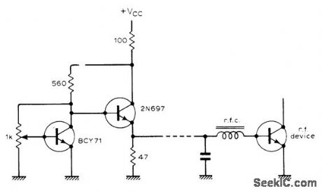
Two-transistor supply using PNP silicon transistor as amplified diode variable-voltage source gives improved-performance transistor RF power amplifier op-erating in class AB Iinear mode. Transistor types are not critical, Output impedance of bias source is about 1 ohm, and output voltage changes only up to 3 1/2 for ±2.5 V change in input voltage Vcc.-C. P, Bartram, Bias Supply for R,F. Power Amplifiers, Wireless World, April 1976,p61. (View)
View full Circuit Diagram | Comments | Reading(707)
1_kHz_SQUARE_WAVE_OSCILLATOR
Published:2009/6/25 21:22:00 Author:Jessie
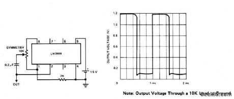
View full Circuit Diagram | Comments | Reading(1164)
R_C_OSCILLATOR
Published:2009/6/25 21:21:00 Author:Jessie
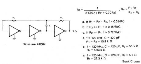
View full Circuit Diagram | Comments | Reading(1241)
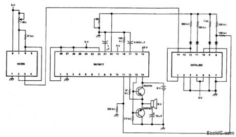
FOUR_CHANNEL_DATA_ACQUlSITION_SYSTEM
Published:2009/6/25 21:20:00 Author:Jessie
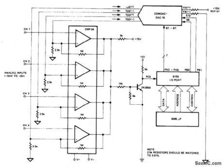
View full Circuit Diagram | Comments | Reading(1080)
SIREN_SPACE_WAR_PHASQR_GUN
Published:2009/6/25 21:13:00 Author:May
The one shot and decay functions could be added to make an ideal phasor gun sound. (View)
View full Circuit Diagram | Comments | Reading(1152)
STEREO_REVERB_ENHANCEMENT_SYSTEM
Published:2009/6/25 21:12:00 Author:May
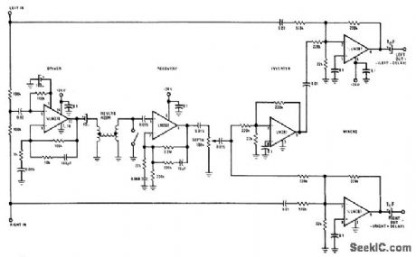
The system can be used to synthesize a stereo effect from a monaural source such as AM radio or FM-mono broadcast, or it can be added to an existing stereo (or quad) system where it produces an exciting opening up special effect that is truly impressive. (View)
View full Circuit Diagram | Comments | Reading(1145)
TRIAC_TRIGGER
Published:2009/6/25 21:21:00 Author:Jessie
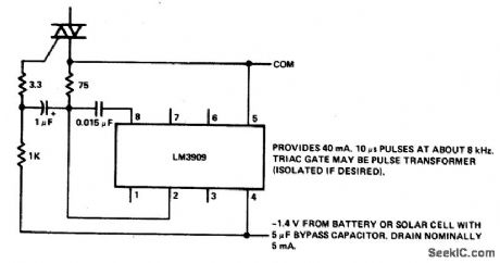
View full Circuit Diagram | Comments | Reading(0)
POSITIVE_INPUT/NEGATIVE_OUTPUT_CHARGE_PUMP
Published:2009/6/25 21:12:00 Author:May

A simple means of generating a low-power voltage supply of opposite polarity from the main supply. Self oscillating driver produces pulses at a repetition frequency of 100 kHz.When the VMOS device is off, capacitor C is charged to the positive supply. When the VMOS transistor switches on, C delivers a negative voltage through the series diode to the output. The zener serves as a dissipative regulator. (View)
View full Circuit Diagram | Comments | Reading(1090)
SOUND_OPERATED_TWO_WAY_SWITCH
Published:2009/6/25 21:20:00 Author:Jessie
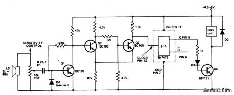
This circuit operates a relay each time a sound of sufficient intensity is made, thus one clap of the hands will switch it one way, a second clap will revert the circuit to the origi-nal condition. Q2 and Q3 form a Schmitt trigger. TheJK flip-flop is used as a bistable whose output changes state every time a pulse is applied to the clock input (pin 12). Q4 allows the output to drive a relay. (View)
View full Circuit Diagram | Comments | Reading(2836)
ULTRA_PRECISE_LONG_TIME_DELAY_RELAY
Published:2009/6/25 21:12:00 Author:May

Circuit NotesPredictable time delays from as low as 0.3 milliseconds to over 3 minutes are obtainable without resorting to a large value electrolytic-type timing capacitor. Instead, a stable low leakage paper or mylar capacitor is used and the peak point urrent of the timing UJT (Q1) is effectively reduced, so that a large value emit-ter resistor (R1) may be substituted. (View)
View full Circuit Diagram | Comments | Reading(885)
POSITIVE_EDGE_DIFFERENTIATOR
Published:2009/6/25 21:19:00 Author:Jessie
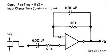
View full Circuit Diagram | Comments | Reading(1089)
200_MHz_CASCODE
Published:2009/6/25 21:12:00 Author:May

JFETs give low cross modulation, large signal-handling ability, and AGC action controlledby biasing upper cascode JFET. Neutralization is not needed.- FET Databook, National Semiconductor, Santa Clara, CA, 1977, p 6-26-6-36. (View)
View full Circuit Diagram | Comments | Reading(708)
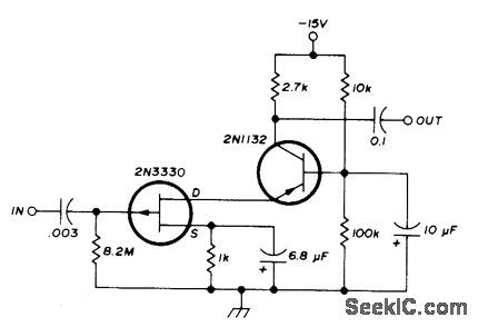
FET_BIPOLAR_SOURCE_FOLLOWER
Published:2009/6/25 21:12:00 Author:May

Used where source follower with high output-voltage swing and voltage gain close to unity is re-quired. Circuit has constant-current bias supply.Combination of unipolar and bipolar transistors gives desirable amplifying features of each solid-state device,-I. M. Gottlieb, A New Look at Solid-State Amplifiers, Ham Radio, Feb. 1976, p16-19. (View)
View full Circuit Diagram | Comments | Reading(1020)
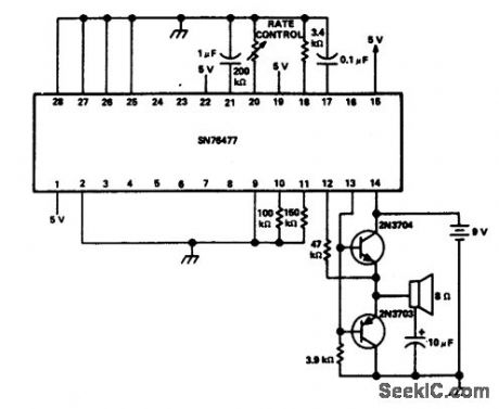
PROGRAMMABLE_BIRD_SOUNDS
Published:2009/6/25 21:11:00 Author:May
View full Circuit Diagram | Comments | Reading(706)
CASCODE
Published:2009/6/25 21:16:00 Author:Jessie
Combination of unipolar and bipolartransistors gives desirable amplifying fea-tures of each solid-state device. Ideal for use whh tuned circuits in audio, video, IF, and RF applications.-I. M. Gottlieb, A New Look at Solid-State Amplifiers, Ham fladio, Feb. 1976, p16-19. (View)
View full Circuit Diagram | Comments | Reading(1222)
NEGATIVE_EDGE_DIFFERENTIATOR
Published:2009/6/25 21:16:00 Author:Jessie

View full Circuit Diagram | Comments | Reading(1177)
UNITY_GAIN_VOLTAGE_FOLLOWER
Published:2009/6/25 21:16:00 Author:Jessie
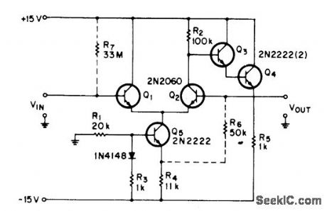
Mea-sured galnis 0.0997 V/V with an error of ±0.1% over ±1.5V swihg Circuit has infinite inputimpedance and zero bias current,Addition of dashed components to simple voltage-follower design gives near-perfect performance.-C. Andren, The Ideal Voltage Follower, EEE Magazine, Jan. 1971, p 63-64. (View)
View full Circuit Diagram | Comments | Reading(727)
TAPE_RECORDER
Published:2009/6/25 21:15:00 Author:Jessie
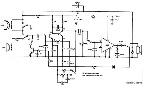
Complete record/playback cassette tape machine amplifier. Two of the transistors act as signal amplifiers, with the third used for automatic level control during the record mode. (View)
View full Circuit Diagram | Comments | Reading(1895)
| Pages:1301/2234 At 2013011302130313041305130613071308130913101311131213131314131513161317131813191320Under 20 |
Circuit Categories
power supply circuit
Amplifier Circuit
Basic Circuit
LED and Light Circuit
Sensor Circuit
Signal Processing
Electrical Equipment Circuit
Control Circuit
Remote Control Circuit
A/D-D/A Converter Circuit
Audio Circuit
Measuring and Test Circuit
Communication Circuit
Computer-Related Circuit
555 Circuit
Automotive Circuit
Repairing Circuit