
Circuit Diagram
Index 1315
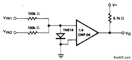
OPPOSITE_POLARITY_INPUT_VOLTAGE_COMPARATOR
Published:2009/6/25 1:48:00 Author:May
View full Circuit Diagram | Comments | Reading(622)
MICROPOWER_DOUBLE_ENDED_LIMIT_DETECTOR
Published:2009/6/25 1:47:00 Author:May
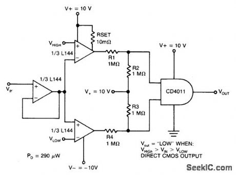
The detector uses three sections of an L144 and a DC4011 type CMOS NAND gate to make a very low power voltage monitor. If the input voltage, VIN, is above VHIGH or below VLOW, the output will be a logical high. If (and only if) the input is between the limits will the output be low. The 1 megohm resistors RI, R2, R3, and R4 translate the bipolar ±10V swing of the op amps to a 0 to 10V swing acceptable to the ground-referenced CM0S logic. (View)
View full Circuit Diagram | Comments | Reading(705)
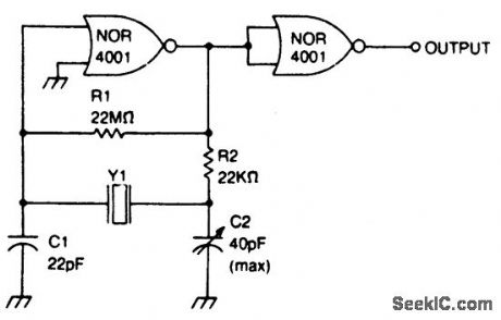
CMOS_CRYSTAL_OSCILLATOR
Published:2009/6/25 1:47:00 Author:May
Circuit Notes
This circuit has a frequency range of 0.5 MHz to 2.0 MHz. Frequency can be adjusted to a precise value with trimmer capacitor C2. The second NOR gate serves as an output buffer. (View)
View full Circuit Diagram | Comments | Reading(2298)
PHOTOMULTIPLIER_CIRCUIT
Published:2009/6/25 1:46:00 Author:May
This circuit is typical of the way that a photomultiplier tube is used. The circuit shown is ac coupled,but if dc coupling is needed,the capacitor can be omitted and a suitable interfacing method used,A typical tube is the widely available 931/931A. (View)
View full Circuit Diagram | Comments | Reading(1382)
FLOODLAMP_POWER_CONTROL
Published:2009/6/25 1:44:00 Author:May
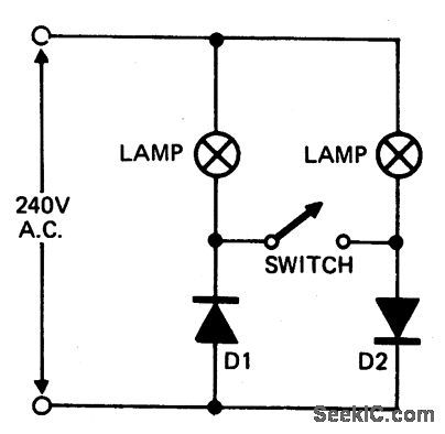
When setting up photographic floodlamps, it is sometimes desirable to operate the lamps at lower power levels until actually ready to take the photograph. The circuit allows the lamps to operate on half cycle power when the switch is open, and full power, when the switch is closed. The diodes D1 and D2 should have a 400 volt PIV rating at 5 amps. (View)
View full Circuit Diagram | Comments | Reading(646)
WINDOW_COMPARATOR_1
Published:2009/6/25 1:44:00 Author:May
View full Circuit Diagram | Comments | Reading(836)
NEGATIVE_VOLTAGE_SUPPLY
Published:2009/6/25 1:43:00 Author:May
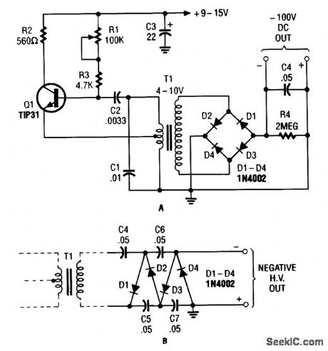
The combination Hartley oscillator/step-up transformer shown in A can generate significant negative high voltage, especially if the voltage output of the transformer is multiplied by the circuit. (View)
View full Circuit Diagram | Comments | Reading(906)
INVERTING_COMPARATOR_WITH_HYSTERESIS
Published:2009/6/25 1:43:00 Author:May
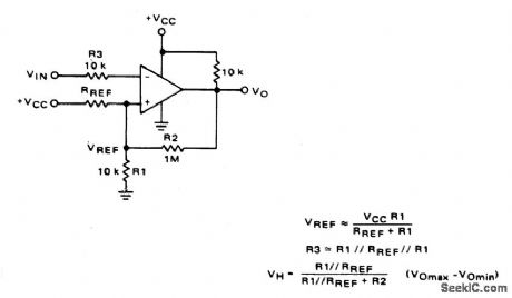
View full Circuit Diagram | Comments | Reading(1594)
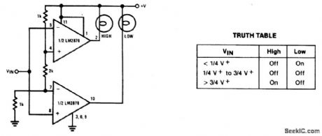
WINDOW_COMPARATOR_DRIVING_HIGH_LOW_LAMPS
Published:2009/6/25 1:40:00 Author:Jessie
View full Circuit Diagram | Comments | Reading(0)
COMPLE_ME_NTARY_LIGHTING_CONTROL
Published:2009/6/25 1:43:00 Author:May
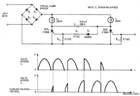
This lighting-control unit will fade out one lamp while simultaneously increasing the light output of another. The two loads track each other accurately without adjustments. The gate of SCR1, a silicon-controlled rectifier, is driven from a standard phase-control circuit, based, for example, on a unijunction transistor or a diac. It controls the brightness of lamp L1 directly. Whenever SCR1 is not on, a small current flows through L1, D1, and R1, permitting SCR2 to fire. When SCR1 turns on, current flow ceases through D1 and R1; the energy stored in C1 produces a negative spike that turns SCR2 off. (View)
View full Circuit Diagram | Comments | Reading(769)
NONINVERTING_COMPARATOR_WITH_HYSTERESIS
Published:2009/6/25 1:42:00 Author:May
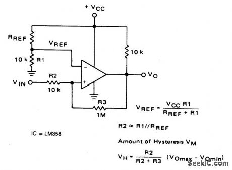
View full Circuit Diagram | Comments | Reading(2990)
THIRD_OVERTONE_CRYSTAL_OSCILLATOR
Published:2009/6/25 1:42:00 Author:May
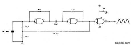
Circuit NotesThis circuit uses a 74500 Schottky TTL gate; no inductors are required. (View)
View full Circuit Diagram | Comments | Reading(1072)
HIGH_POWER_CONTROLFOR_SENSITIVE_CONTACTS
Published:2009/6/25 1:40:00 Author:Jessie
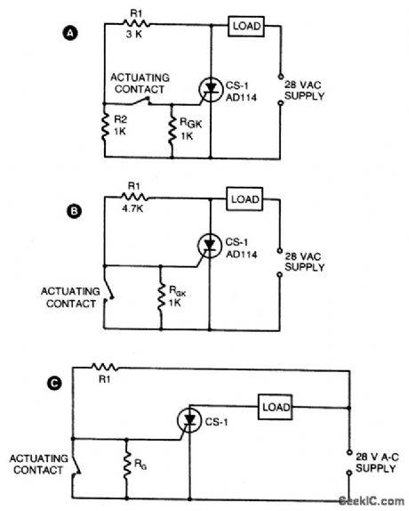
Two simple arrangements for resistive loads are shown in A & B. The circuit in A will provide load power when the actuating contact is closed, and no power when the contact is open. B provides the reierse of this action-power being supplied to the load when the contact is open with no load power when the contact is closed. If desired, both circuits can be made to latch by operating with dc instead of the indicated ac supply. In both of these circuits, voltage across the sensitive contacts is under 5 volts, and contact current is below 5 mA. For inductive loads, R1 would normally be returned to the opposite side of the load as shown in C. (View)
View full Circuit Diagram | Comments | Reading(0)
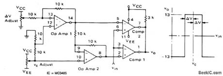
COMPARATOR_WITH_TIME_OUT
Published:2009/6/25 1:42:00 Author:May
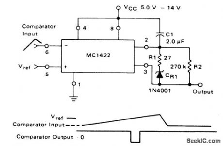
The MC1422 is used as a comparator with the capability of a timing output pulse when the inverting input (Pin 6) is ≥the noninverting input (Pin 5). The frequency of the pulses for the values of R2 and C1 as shown is approxi-mately 2.0 Hz, and the pulse width 0.3 ms. (View)
View full Circuit Diagram | Comments | Reading(662)
WINDOW_COMPARATOR
Published:2009/6/25 1:39:00 Author:Jessie

This circuit gives an output (which in this case is 0V) when an input voltage lies in be-tween two specified voltages. When it is out-side this window, the output is positive. The two op amps are used as voltage comparators. When Vin is more positive than Vref (upper) the output of IC1 is positive and Dl is forward biased. Otherwise the output is negative, D1 reverse biased and hence Vout is 0V. Similarly, when Vin is more negative than Vref (lower), the output of IC2 is positive; D2 is forward biased and this Vout is positive. Otherwise Vout is 0V. When Vin lies within the window set by the reference voltages, Vout is 0V. (View)
View full Circuit Diagram | Comments | Reading(0)
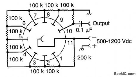
HIGH_LOW_LIMIT_ALARM
Published:2009/6/25 1:38:00 Author:Jessie
View full Circuit Diagram | Comments | Reading(1272)
WINDOW_COMPARATOR_DRIVING_HIGH_LOW_LAMPS
Published:2009/6/25 1:40:00 Author:May
View full Circuit Diagram | Comments | Reading(991)
HIGH_POWER_CONTROLFOR_SENSITIVE_CONTACTS
Published:2009/6/25 1:40:00 Author:May
Two simple arrangements for resistive loads are shown in A & B. The circuit in A will provide load power when the actuating contact is closed, and no power when the contact is open. B provides the reierse of this action-power being supplied to the load when the contact is open with no load power when the contact is closed. If desired, both circuits can be made to latch by operating with dc instead of the indicated ac supply. In both of these circuits, voltage across the sensitive contacts is under 5 volts, and contact current is below 5 mA. For inductive loads, R1 would normally be returned to the opposite side of the load as shown in C. (View)
View full Circuit Diagram | Comments | Reading(1233)
WINDOW_COMPARATOR
Published:2009/6/25 1:39:00 Author:May
This circuit gives an output (which in this case is 0V) when an input voltage lies in be-tween two specified voltages. When it is out-side this window, the output is positive. The two op amps are used as voltage comparators. When Vin is more positive than Vref (upper) the output of IC1 is positive and Dl is forward biased. Otherwise the output is negative, D1 reverse biased and hence Vout is 0V. Similarly, when Vin is more negative than Vref (lower), the output of IC2 is positive; D2 is forward biased and this Vout is positive. Otherwise Vout is 0V. When Vin lies within the window set by the reference voltages, Vout is 0V. (View)
View full Circuit Diagram | Comments | Reading(1371)
HIGH_LOW_LIMIT_ALARM
Published:2009/6/25 1:38:00 Author:May
View full Circuit Diagram | Comments | Reading(0)
| Pages:1315/2234 At 2013011302130313041305130613071308130913101311131213131314131513161317131813191320Under 20 |
Circuit Categories
power supply circuit
Amplifier Circuit
Basic Circuit
LED and Light Circuit
Sensor Circuit
Signal Processing
Electrical Equipment Circuit
Control Circuit
Remote Control Circuit
A/D-D/A Converter Circuit
Audio Circuit
Measuring and Test Circuit
Communication Circuit
Computer-Related Circuit
555 Circuit
Automotive Circuit
Repairing Circuit