
Circuit Diagram
Index 1307
TTLLOGIC_TESTER
Published:2009/6/25 4:26:00 Author:May
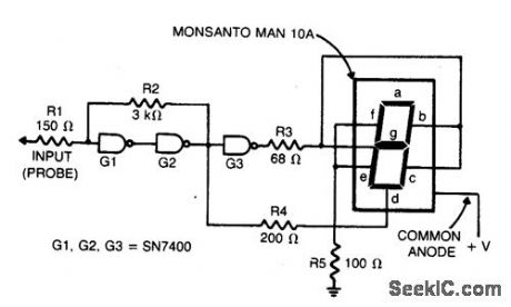
Gates GI and G2 together with resistors RI and R2 form a simple voltage monitor that has a trip point of 1.4 volts. Gate G3 is simply an inverter. The display section of the tester consists of a common anode alphanumeric LED and current-limiting resistors. It indicates whether the input voltage is above or below 1.4 V, and displays a H or a L (for high or low logic-level) respectively. (View)
View full Circuit Diagram | Comments | Reading(786)
AUDIO_RF_SIGNAL_TRACER_PROBE
Published:2009/6/25 4:24:00 Author:May
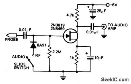
This economical signal tracer is useful for servicing and alignment work in receivers and low power transmitters. When switched to RF, the modulation on any signal is detected by the diode and amplified by the FET. A twin-core shielded lead can be used to connect the probe to an amplifier and to feed 6 volts to it. (View)
View full Circuit Diagram | Comments | Reading(3189)
PRECISION_CURRENT_SINK
Published:2009/6/25 4:18:00 Author:May
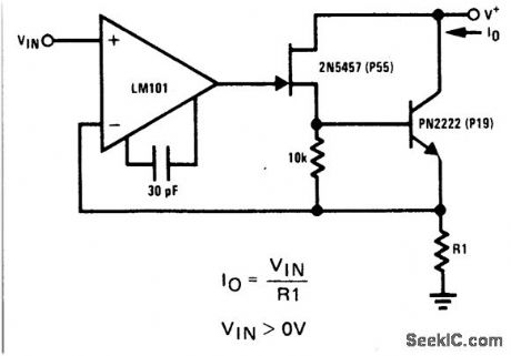
Circuit Notes
The 2N5457 JFET and PN2222 bipolar have inherently high output impedance. Using R1 as a current sensing resistor to provide feedback to the LM101 op amp provides a large amount of loop gain for negative feedback to enhance the true current sink nature of this circuit. For small current values, the 10 K re-sistor and PN2222 may be eliminated if the source of the JFET is connected to R1. (View)
View full Circuit Diagram | Comments | Reading(0)
SIMPLE_LOGIC_PROBE
Published:2009/6/25 4:17:00 Author:May
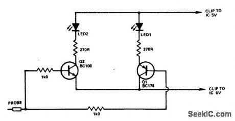
If the probe is connected to logic 0, Q1 will be turned on lighting D1. At logic 1, Q2 will be turned on lighting D2. For Q1 and Q2 any NPN or PNP transistors will do.Similarly, D1 and D2 can be any LEDs. (View)
View full Circuit Diagram | Comments | Reading(1378)
NEGATIVE_TO_POSITIVE_SUPPLY_LOGIC_LEVEL_SHIFTER
Published:2009/6/25 3:13:00 Author:May
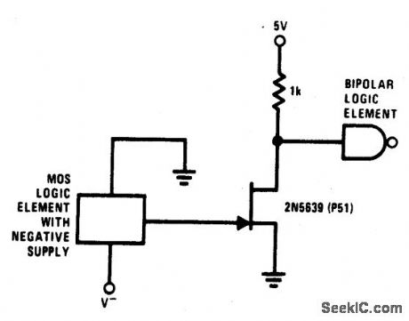
This simple circuit provides for level shifting from any logic function (such as MOS) operating from minus to ground supply to any logic level (such as TTL) operating from a plus to ground supply. The 2N5639 provides a low rdc (ON) and fast switching times. (View)
View full Circuit Diagram | Comments | Reading(921)
SELF_OSCILLATING_FLYBACK_CONVERTER
Published:2009/6/25 2:43:00 Author:May
A low-power converter suitable for deriving a higher voltage from a main system rail in an on-board application. With the transformer shown, the operating frequency is 250kHz. Z1 serves as a dissipative voltage regulator for the output and also clips the drain voltage to a level below the rated VMOS breakdon boltage. (View)
View full Circuit Diagram | Comments | Reading(1875)
BCD_TO_ANALOG_CONVERTER
Published:2009/6/25 2:05:00 Author:May
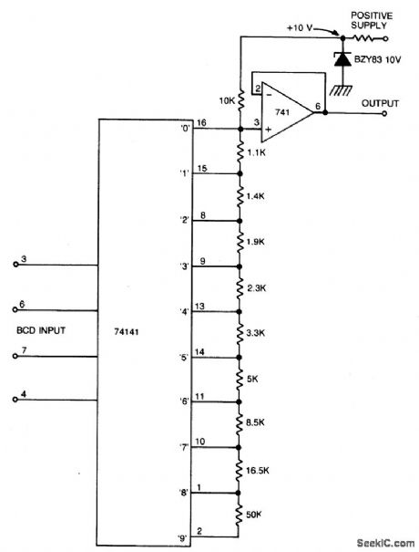
This circuit will convert four-bit BCD into a variable voltage from 0-9 V in 1 V steps. The SN74141 is a Nixie driver, and has ten open-collector outputs. These are used to ground a selected point in the divider chain determined by the BCD code at the input, and so produce a corresponding voltage at the output. Accuracy of the circuit depends on the tolerance of the resistors and the accuracy of the reference vol-tage. However, presets can be used in the di-viderchain, with correct calibration. The 741 is used as a buffer. (View)
View full Circuit Diagram | Comments | Reading(1992)
100_K_MEGOHM_DC_PROBE
Published:2009/6/25 4:10:00 Author:Jessie
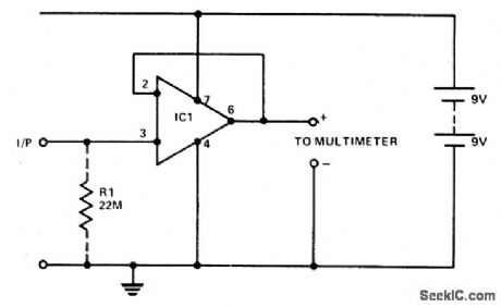
A 741 op amp is used with t00% ac and dc feedback to provide a typical input impedance of 1011 ohm and unity gain. To avoid hum and rf pickup the input leads should be kept as short as possible and the circuit should be mounted in a small grounded case. Output leads may belong since the output impedance of the circuit is a fraction of an ohm. With no input the output level is indeterminate. Including RI in the cir-cuit through lowers the input impedance to 22 M. (View)
View full Circuit Diagram | Comments | Reading(1244)
RF_PROBE_FOR_VOM
Published:2009/6/25 4:09:00 Author:Jessie
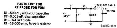
This probe makes possible relative measurements of rf voltages to 200 MHz on a 20,000 ohms-per-volt multimeter.Rf voltage must not exceed the breakdown rating of the IN4149-approximately 100 V. (View)
View full Circuit Diagram | Comments | Reading(1142)
CMOS_LOGIC_PROBE
Published:2009/6/25 4:07:00 Author:Jessie

The logic probe can indicate four input states, as follows: floating input-all LEDs off; logic 0 input-D2 switched on (D3 will briefly flash on); logic 1 input-Dl switched on; pulsing input-D3 switched on, or pulsing in the case of a low frequency input signal (one or both of the other indicators will switch on, showing if one input state predominates). (View)
View full Circuit Diagram | Comments | Reading(0)
INJECTOR_TRACER
Published:2009/6/25 4:06:00 Author:Jessie
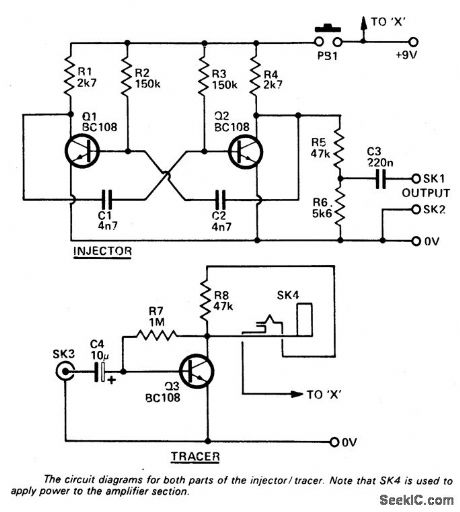
The unit has a separate amplifier and oscillator section allowing them to be used sepa-rately if need be. The injector is a multivibrator running at 1 kHz, with R5 and R6 dividing down the output to a suitable level (≈1V). The tracer is a single-stage amplifier that drives the high impedance earpiece. C4 decouples the input. (View)
View full Circuit Diagram | Comments | Reading(1974)
SIGNAL_INJECTOR_TRACER
Published:2009/6/25 4:04:00 Author:Jessie
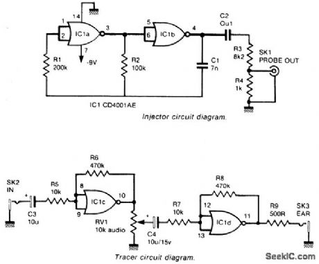
The injector is a CMOS oscillator with period approximately equal to 1.4 x C1 x R2 seconds. The values are given for 1 kHz opera-tion. Resistors R3 and R4 divide the output to 1 V. Whereas the oscillator employs the gates in their digital mode, the tracer used them in a linear fashion by applying negative feedback from output to input. They are used in much the same way as op amps. The circuit uses positiveground. It offers an advantage at the earphone output because one side of the earphone must be connected to ground via the case. Use of a positive ground allows the phone to be driven by the two N-channel transistors inside the CD4001 which are arranged in parallel and are thus able to handle more current for better volume. (View)
View full Circuit Diagram | Comments | Reading(3525)
LOGIC_PROBE_YIELDS_THREE_DISCRETE_STATES
Published:2009/6/25 4:02:00 Author:Jessie
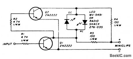
The circuit uses a dual LED. When power is applied to the probe through the power leads, and the input is touched to a low level or ground, Q1 is cut off. This will cause Q2 to conduct since the base is positive with respect to the emitter. With Q1 cut off and Q2 con-ducting, the greendiode ofthe dual LED will be forward biased, yielding a green output.Touching the probe tip to a high level will cause Q1 and Q2 to complement, and the red diode will be forward biased, yielding a red output from the LED. An alternating signal will cause alternating conduction of the red and green diodes and willyield an indication approxi-mately amber. In this manner, both static and dynamic signals can be traced with the logic probe. (View)
View full Circuit Diagram | Comments | Reading(1523)
CURRENT_SOURCE
Published:2009/6/25 3:52:00 Author:May
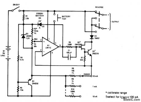
Circuit Notes
This precision current source has 10 μA to 10 mA ranges with output compliance or 30V to -5V. Output current is fully adjustable oneach range with a calibrated, ten-turn potentiometer. Error light indicates saturation. (View)
View full Circuit Diagram | Comments | Reading(2989)
CURRENT_MONITOR
Published:2009/6/25 3:31:00 Author:May
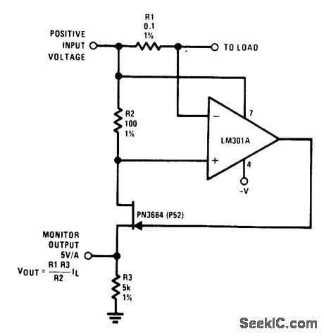
Circuit Notes
R1 senses current flow of a power supply. The JFET is used as a buffer because ID = Is; therefore the output monitor voltage accu-rately reflects the power supply current flow. (View)
View full Circuit Diagram | Comments | Reading(0)
NANOAMPERE_SENSING_CIRCUIT_WITH_100_MEGOHM_INPUT_IMPEDANCE
Published:2009/6/25 3:29:00 Author:May
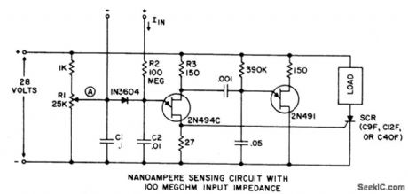
Circuit Notes
The circuit may be used as a sensitive current detector or as a voltage detector having high input impedance. RI is set so that the voltage at point (A) is Vz to 3A volts below the level that fires the 2N494C. A small input cur-rent (Iin) of only 40 nanoamperes will charge C2 and raise the voltage at the emitter to the firing level. When the 2N494C fires, both capacitors, C1 and C2, are discharged through the 27 ohm resistor, which generates a positive pulse with sufficient amplitude to trigger a con-trolled rectifier (SCR), or other pulse sensitive circuitry. (View)
View full Circuit Diagram | Comments | Reading(0)
NANO_AMMETER
Published:2009/6/25 3:25:00 Author:May
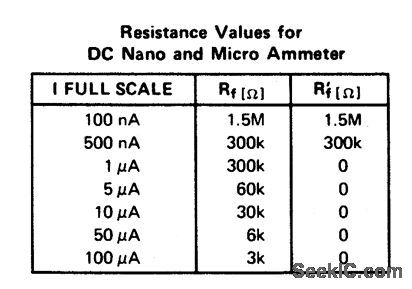
The complete meter amplifier is a differen-tial current-to-voltage converter with input pro-tection, zeroing and full scale adjust provisions, and input resistor balancing for minimum offset voltage. (View)
View full Circuit Diagram | Comments | Reading(0)
CURRENT_MONITOR
Published:2009/6/25 3:31:00 Author:Jessie
Circuit Notes
R1 senses current flow of a power supply. The JFET is used as a buffer because ID = Is; therefore the output monitor voltage accu-rately reflects the power supply current flow. (View)
View full Circuit Diagram | Comments | Reading(1698)
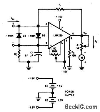
PICO_AMMETER
Published:2009/6/25 3:22:00 Author:May
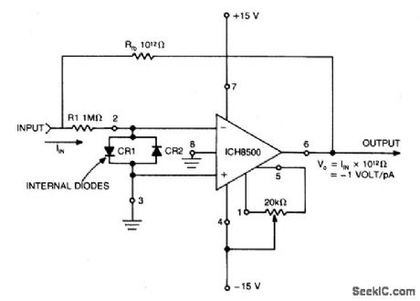
Circuit Notes
A very sensitive pico ammeter (-1V/pA) employs the amplifier in the inverting or cur-rent summing mode. Care must be taken to eliminate stray currents from flowing into the current summing mode. It takes approximately 5 for the circuit to stabilize to within 1% of its final output voltage after a step function of input current has been applied. The internal diodes CR1 and CR2 together with external resistor R1 to protect the input stage of the amplifier from voltage transients. (View)
View full Circuit Diagram | Comments | Reading(4080)
1AND_GATE
Published:2009/6/25 3:18:00 Author:May
View full Circuit Diagram | Comments | Reading(667)
| Pages:1307/2234 At 2013011302130313041305130613071308130913101311131213131314131513161317131813191320Under 20 |
Circuit Categories
power supply circuit
Amplifier Circuit
Basic Circuit
LED and Light Circuit
Sensor Circuit
Signal Processing
Electrical Equipment Circuit
Control Circuit
Remote Control Circuit
A/D-D/A Converter Circuit
Audio Circuit
Measuring and Test Circuit
Communication Circuit
Computer-Related Circuit
555 Circuit
Automotive Circuit
Repairing Circuit