
Circuit Diagram
Index 1306
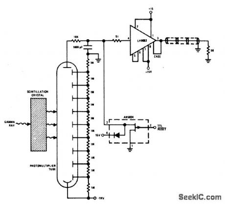
GAMMA_RAY_PULSE_INTEGRATOR
Published:2009/6/25 5:10:00 Author:May
View full Circuit Diagram | Comments | Reading(726)
DIODE_TESTER
Published:2009/6/25 20:48:00 Author:Jessie
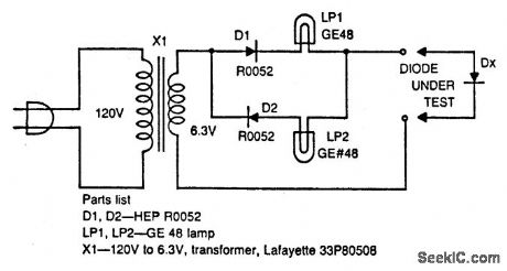
The circuit tests whether or not a diode is open, shorted, or functioning correctly. If lamp A lights, the diode under test is functional. When lamp B is lit, the diode is good but connected backwards. When both lamps are lit, the diode is shamed, and it is open if neither lamp is lit. (View)
View full Circuit Diagram | Comments | Reading(1487)
WIDEBAND_RADIATION_MONITOR
Published:2009/6/25 5:09:00 Author:May
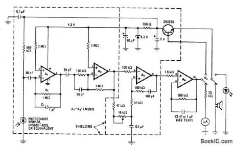
A sensitive radiation monitor may be sim-ply constructed with a large-area photodiode and a quad operational amplifier. Replacing the glass window of the diode with Mylar foil wili shield it from light and infrared energy,enabbling it to respond to such nuclear radiation as alpha and beta particles and gamma rays. A4 integrates the output of A3 In order to drive amlcroammeter,Al microfarad capacitor isused in the integratingnetwork.A lower value,say,33 nanofarads,will make it possible todrive a small loudspeaker (50-hertz output signal) or light-emitting diode. (View)
View full Circuit Diagram | Comments | Reading(1536)
DOSAGE_RATE_METER
Published:2009/6/25 5:07:00 Author:May

A commercial diode is the detector in this highly accurate radiation monitor. The lowdrift FET-input op amp amplifies detector current to a usable level, and the chopper-stabilized amplifier then provides additional gain while minimizing any error caused by ambient-temperature fluctuations. Gain is adjusted so that the output voltage is 1% of incident radia-tion intensity in rads per minute; therefore voltage can be displayed on 3 1/2 digit DVM for direct reading of dosage rate. Output voltage from the monitor is linearly proportional to radiation intensity at the diode. (View)
View full Circuit Diagram | Comments | Reading(1444)
VERSATILE_TWO_PHASE_PULSE_GENERATOR
Published:2009/6/25 4:47:00 Author:May
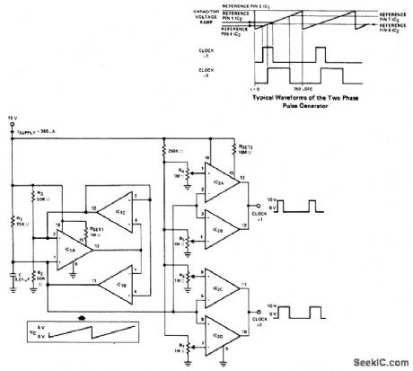
Two-phase clock generator uses two L161s to generate pulses of adjustable widths and phase relationships. Ramp generator feeds two variable window comparators formed by IC2A-IC2B and IC2C-IC2D respectively. (View)
View full Circuit Diagram | Comments | Reading(753)
555_TIMER_OSCILLATOR
Published:2009/6/25 4:46:00 Author:May
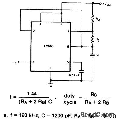
View full Circuit Diagram | Comments | Reading(990)
PULSE_GENERATOR_WITH_25%_DUTY_CYCLE_
Published:2009/6/25 4:45:00 Author:May
View full Circuit Diagram | Comments | Reading(852)
PULSE_GENERATOR_3
Published:2009/6/25 4:45:00 Author:May
View full Circuit Diagram | Comments | Reading(579)
FREE_RUNNING_OSCILLATOR_
Published:2009/6/25 4:44:00 Author:May
View full Circuit Diagram | Comments | Reading(782)
PULSE_GENERATOR_2
Published:2009/6/25 4:43:00 Author:May
View full Circuit Diagram | Comments | Reading(600)
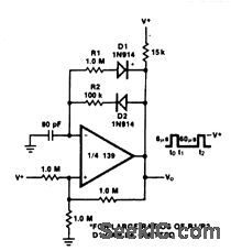
PULSE_GENERATOR_1
Published:2009/6/25 4:43:00 Author:May
View full Circuit Diagram | Comments | Reading(1355)
UNIJUNCTION_TRANSISTOR_PULSE_GENERATORS
Published:2009/6/25 4:42:00 Author:May
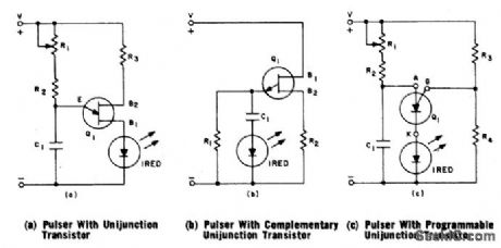
View full Circuit Diagram | Comments | Reading(844)
PROGRAMMABLE_PULSE_GENERATOR
Published:2009/6/25 4:42:00 Author:May
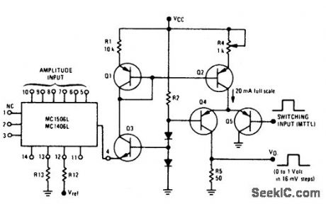
Fast rlse and fall times requlre the use of high speed switching transistors for the differential patr,Q4 and Q5.Linear ramps and slnewaves may be generated by the appropriatereference input. (View)
View full Circuit Diagram | Comments | Reading(0)
SINGLE_OP_AMP_OSCILLATOR
Published:2009/6/25 4:40:00 Author:May
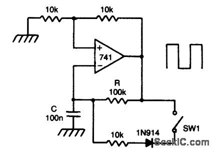
This circuit has a Schmitt trigger and in-tegrator built around one op amp. Timing is controlled by the RC network. Voltage at the inverting input follows the RC charging expo-nential within the upper and lower hysteresis levels. By closing the switch SWt, the dis-charge time of the capacitor becomes ten times as fast as the rise time. Thus a square wave with an 10:1 mark space ratio is generated. (View)
View full Circuit Diagram | Comments | Reading(1359)
400_V,60_W_PUSH_PULL_DC_DC_CONVERTER
Published:2009/6/25 4:40:00 Author:May
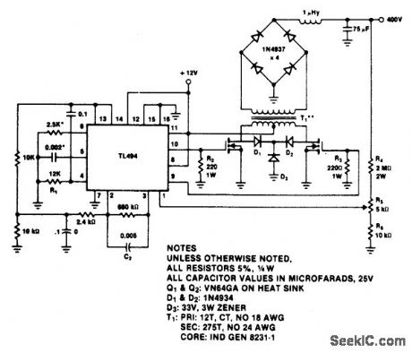
Circuit Notes
The TL494 switching regulator governs the operating frequency and regulates output voltage, Switching frequency approximately 100 kHz for the values shown。Output regulation IS typically 1.25% from no-load to full 60 W。 (View)
View full Circuit Diagram | Comments | Reading(5101)
REGULATED_DC_TO_DC_CONVERTER
Published:2009/6/25 4:38:00 Author:May
Circuit Notes
Low power dc to dc converter obtained by adding a flyback circuit to a square wave oscil-lator. Operating frequency is 20 kHz to minimize the size of L1 and C2. Regulation is achieved by zener diode D2. Maximum current available before the convener drops out of reg-ulation is 5.5 rnA. (View)
View full Circuit Diagram | Comments | Reading(900)
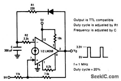
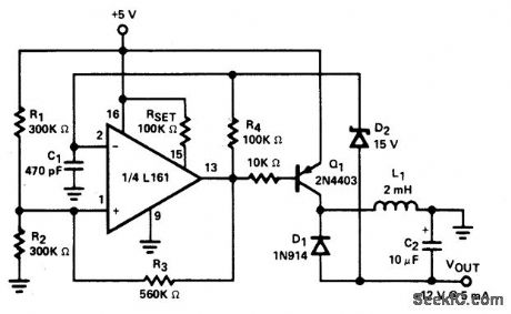
PULSE_GENERATOR
Published:2009/6/25 4:37:00 Author:May

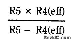
The duty cycle ofthe output pulse is equalto R4/(R4+R5)×100%.For duty cycles ofless than 50%,D1 can be eliminated and R2raised according to the following formula∶
R4(actual)=
R4c(eff) IS the effective value ofR4 in the circuitand R4(actual)IS the actual value used;R4(ac-tual)will always be larger than R4(eff). (View)
View full Circuit Diagram | Comments | Reading(0)
MINI_POWER_INVERTER_AS_HIGH_VOLTAGELOW_CURRENT_SOURCE
Published:2009/6/25 4:34:00 Author:May
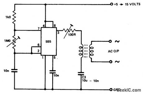
Circuit Notes
The circuit is capable of providing power for portable Geiger counters, dosimeter char-gers, higlt resistance meters, etc. The 555 timer IC is used in its multivibrator mode, the frequency adjusted to optimize the transformer characteristics. When the output of the IC is high, current flows through the limiting resis-tor, the primary coil to charge C3. When the output is low, the current is reversed. With a suitable choice of frequency and C3, a good symmetric output is sustained. (View)
View full Circuit Diagram | Comments | Reading(1167)
DC_TO_DC_SMPS_USING_NE5561_VARIABLE_18_V_to_30_V_OUT_AT_O2_A
Published:2009/6/25 4:32:00 Author:May
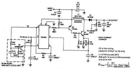
View full Circuit Diagram | Comments | Reading(630)
DC_TO_DC_AC_INVERTER
Published:2009/6/25 4:28:00 Author:May
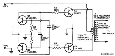
Circuit Notes
This inverter uses no special components such as the torodial transformer used in many inverters. Cost is kept ldw with the use of cheap, readily available components. Essen-tially, it is a power amplifier driven by an asta-ble multivibrator. The frequency is around 1200 Hz which most 50/60 Hz power transfor-mers handle well without too much loss. In-creasing the value of capacitors C1 and C2 will lower the frequency if any trouble is experi-enced. However, rectifier filtering capacitors required are considerably smaller at the higher operating frequency. The two 2N3055 transis-tor should be mounted on an adequately sized heatsink. The transformer should be rated ac-cording to the amount of output power required allowing for conversion efficiency of approxi-mately 60%. (View)
View full Circuit Diagram | Comments | Reading(2579)
| Pages:1306/2234 At 2013011302130313041305130613071308130913101311131213131314131513161317131813191320Under 20 |
Circuit Categories
power supply circuit
Amplifier Circuit
Basic Circuit
LED and Light Circuit
Sensor Circuit
Signal Processing
Electrical Equipment Circuit
Control Circuit
Remote Control Circuit
A/D-D/A Converter Circuit
Audio Circuit
Measuring and Test Circuit
Communication Circuit
Computer-Related Circuit
555 Circuit
Automotive Circuit
Repairing Circuit