
Circuit Diagram
Index 1311
_5_V__36_V_FROM_4_AA_CELLS
Published:2009/6/25 2:28:00 Author:Jessie
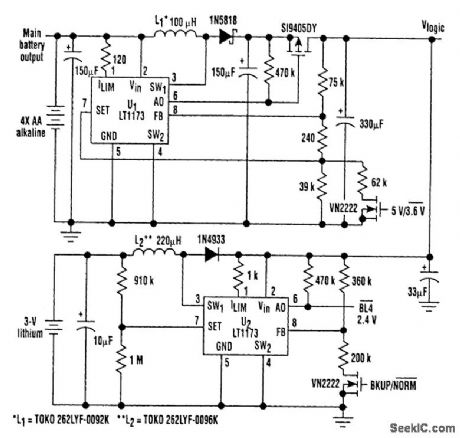
With this unique logic-power-converter design (see the figure), a switchable 3.6 or 5 V at 200 mA can be attained by using four AA cells. The supply incorporates a MOSFET switch that can switch to a lithium backup battery, providing a 3.4-V output when the main battery is dead or removed. The supply consumes only 380 pA under no-load conditions.
The circuit operates in a somewhat novel mode as a step-up/step-down converter. When the cells are fresh (from about 6 V to about 5.2 V), the LT1173's gain block drives the p-channel MOSFET, which turns the circuit into a linear voltage regulator. This might seem inefficient, but the batteries are quick to drop from 6 V to 5 V. With a 5-V input, the efficiency (for the 3.6-V output) is 3.6/5 or 72%, which is reasonable. As the battery-pack drops in voltage, efficiency increases, reaching greater than 90% with a 4.2-V input.
At a point below a 4-V input, the circuit switches to step-up mode. This mode squeezes the bat-teries for all of their available energy. In this case, efficiency runs between 83% at approximately a 4-V input to 73% at a 2.5-V input.
The supply can deliver 200 mA over its entire operational range. In its linear mode of operation, the supply has no current spikes that, because of the fairly high internal resistance of the alkaline cells, can reduce battery life. The topology delivers over 9.3 hours of 3.6-V 200-mA output power, compared to just 7 hours using the traditional flyback topology that is used in other designs. (View)
View full Circuit Diagram | Comments | Reading(847)
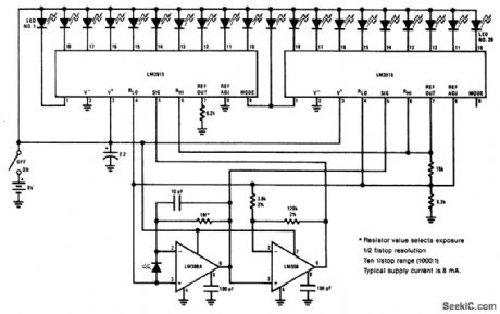
2LIGHT_METER
Published:2009/6/25 2:25:00 Author:May
View full Circuit Diagram | Comments | Reading(0)
LIGHT_INTENSITY_TO_FREQUENCY_CONVERTER
Published:2009/6/25 2:28:00 Author:Jessie
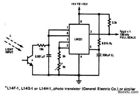
View full Circuit Diagram | Comments | Reading(1561)
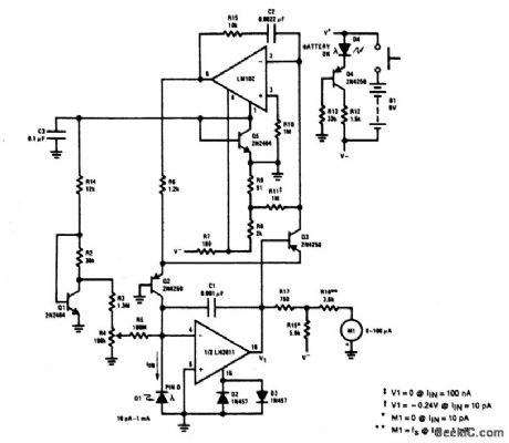
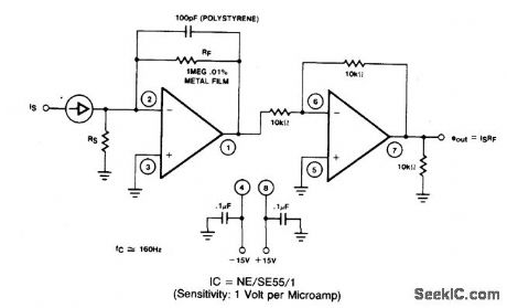
VOLTAGE_TO_CURRENT_CONVERTER
Published:2009/6/25 2:24:00 Author:May
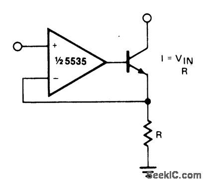
The current out is IOUT≌VIN/R. For negative currents, a PNP can be used and, for better accuracy, a Darlington pair can be substituted for the transistor. With careful design, this cir-cuit can be used to control currents of many amps. Unity gain compensation is necessary. (View)
View full Circuit Diagram | Comments | Reading(0)
PRECISION_PHOTODIODE_COMPARATOR
Published:2009/6/25 2:28:00 Author:Jessie
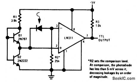
View full Circuit Diagram | Comments | Reading(0)
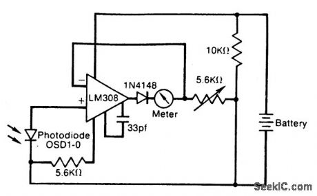
1LIGHT_METER
Published:2009/6/25 2:24:00 Author:May
View full Circuit Diagram | Comments | Reading(720)
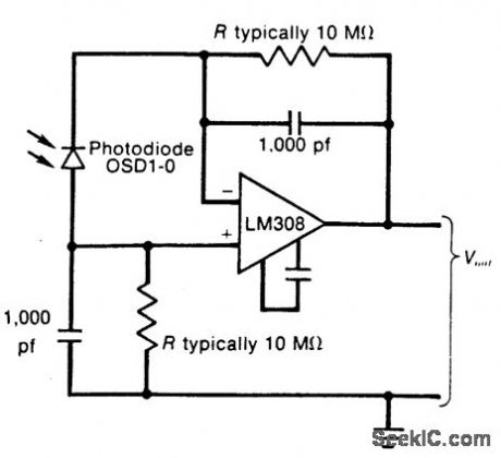
3LIGHT_METER
Published:2009/6/25 2:27:00 Author:Jessie
This light meter has an eight-decade range. Bias current compensation can give input current resolution of better than ±2 pA over 15 ℃ to 55℃. (View)
View full Circuit Diagram | Comments | Reading(1262)
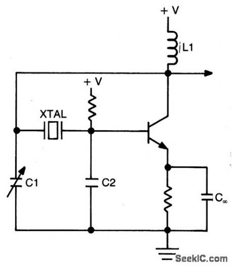
MILLER_OSCILLATOR_CRYSTAL_CONTROLLED
Published:2009/6/25 2:24:00 Author:May
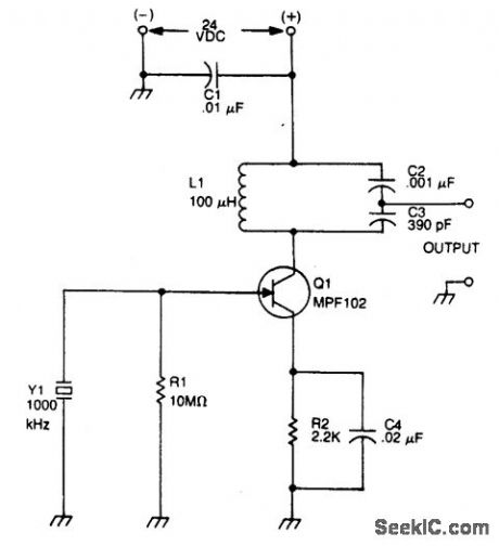
Circuit Notes
The drain of the JFET Miller oscillator is tuned to the resonant frequency of the crystal by an LO tank circuit. (View)
View full Circuit Diagram | Comments | Reading(1462)
PRECISION_CLOCK_GENERATOR
Published:2009/6/25 2:23:00 Author:May
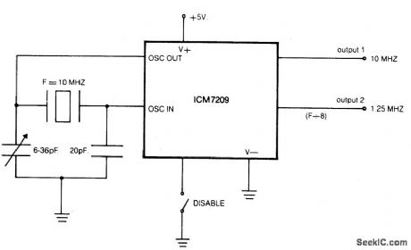
Circuit NotesThe CMOS IC directly drives 5 TTL loads from either of 2 buffered outputs. device operates to 10 MHz and is bipolar, MOS, and CMOS compatible. (View)
View full Circuit Diagram | Comments | Reading(864)
BUTLER_EMITTER_FOLLOWER_OSCILLATOR(20_MHz)
Published:2009/6/25 2:26:00 Author:Jessie
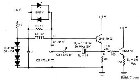
View full Circuit Diagram | Comments | Reading(1219)
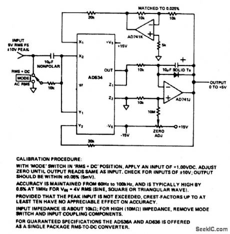
WIDEBAND_HIGH_CREST_FACTOR_RMS_TO_DE_COMVERTER
Published:2009/6/25 2:26:00 Author:Jessie
View full Circuit Diagram | Comments | Reading(1577)
POLARITY_CONVERTER
Published:2009/6/25 2:22:00 Author:May
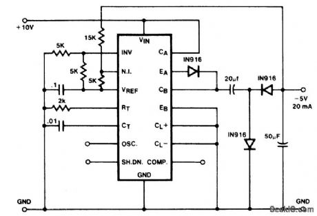
The capacitor-diode output circuit is used here as a polarity converter to generate a -5 volt supply from +15 volts. This circuit is use-ful for an output current of up to 20 mA with no additional boost transistors required. Since the output transistors are current limited, no addi-tional protection is necessary. Also, the lack of an inductor allows the circuit to be stabilized with only the output capacitor. (View)
View full Circuit Diagram | Comments | Reading(1076)
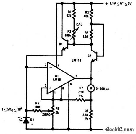
LOGARITHMIC_LIGHT_METER_CIRCUIT
Published:2009/6/25 2:22:00 Author:May
The meter reading is directly proportional to the logarithm of the input light power. The logarithmic circuit behavior arises from the nonlineardiode pnjunction current/voltage relationship. The diode in the amplifier output prevents output voltage from becoming nega-tive (thereby pegging the meter), which may happen at low lightlevels due to amplifier bias currents. R1 adjusts the meter full-scale deflection, enabling the meter to be calibrated. (View)
View full Circuit Diagram | Comments | Reading(1318)
2LIGHT_METER
Published:2009/6/25 2:25:00 Author:Jessie
View full Circuit Diagram | Comments | Reading(1174)
CURRENT_TO_VOLTAGE_CONVERTER_WITH_1_Accuracy
Published:2009/6/25 2:21:00 Author:May
A filter removes the dc component of the rectified ac, which is then scaled to RMS. The output is linear from 40 Hz to 10 kHz or higher. (View)
View full Circuit Diagram | Comments | Reading(919)
LINEAR_LIGHT_METER_CIRCUIT
Published:2009/6/25 2:21:00 Author:May
This circuit uses a low-input-bias op amp to give a steady dc indication of light level. To reduce circuit sensitivity to light, R1 can be reduced, but should not be less than 100 K. The capacitor values in the circuit are chosen to provide a time constant sufficient to filter high-frequency light variations that might arise, for example, from fluorescent lights. (View)
View full Circuit Diagram | Comments | Reading(1526)
UNIVERSAL_LABORATORY_POWER_SUPPLY
Published:2009/6/25 2:21:00 Author:May
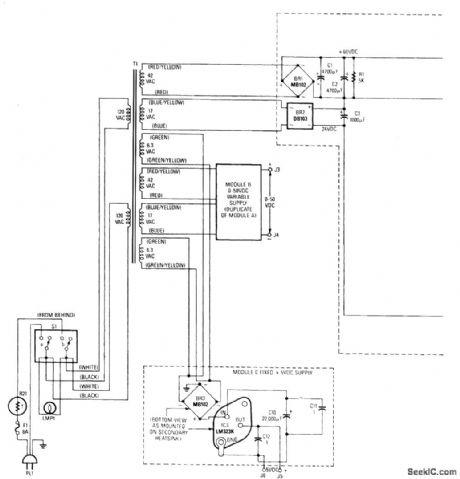
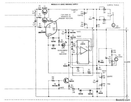
The value of the design lies in the use of IC1,an LM317HVK adjustable serles-pass voltage regulator,for broad-range performance remainder supplies voltage-setting and current limiting functions The input to IC1 comes from the output of BR1,which is filtered by C1 and C2 to about +60Vdc,and the input for current-sense comparator IC2 comes from BR2,which also acts as a negative bias supply for regulation down to ground. The output voltage is determined by∶( VOUT - 1.25 + 1.3 ) /( R15 + R16 ) = 1.25 / R8.Thus,the maximum value from each variable supply board is∶VOUT = ( 1.25 / R8 ) × ( R15 + R16 ) = 50.18 Vdc (View)
View full Circuit Diagram | Comments | Reading(2259)
TUBE_TYPE_CRYSTAL_OSCILLATOR
Published:2009/6/25 2:20:00 Author:May
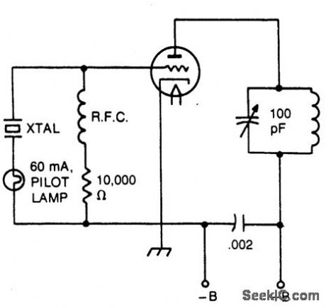
Circuit Notes
The pilot lamp limits current to prevent damage to the crystal. (View)
View full Circuit Diagram | Comments | Reading(870)
AC_TO_DC_CONVERTER
Published:2009/6/25 2:20:00 Author:May
This circuit includes a PMOS enhancement-mode FET input buffer amplifier, coupled to a classical absolute value circuit which essentially eliminates the effect of the forward voltage drop across diodes D1 and D2. (View)
View full Circuit Diagram | Comments | Reading(1954)
PIERCE_HARMONIC_OSCILLATOR(BASIC_CIRCUIT)
Published:2009/6/25 2:20:00 Author:May
Circuit Notes
This circuit operates 10-40 ppm above series resonance. It is a good circuit design with good to very good frequency stability. (View)
View full Circuit Diagram | Comments | Reading(1025)
| Pages:1311/2234 At 2013011302130313041305130613071308130913101311131213131314131513161317131813191320Under 20 |
Circuit Categories
power supply circuit
Amplifier Circuit
Basic Circuit
LED and Light Circuit
Sensor Circuit
Signal Processing
Electrical Equipment Circuit
Control Circuit
Remote Control Circuit
A/D-D/A Converter Circuit
Audio Circuit
Measuring and Test Circuit
Communication Circuit
Computer-Related Circuit
555 Circuit
Automotive Circuit
Repairing Circuit