
Circuit Diagram
Index 1308
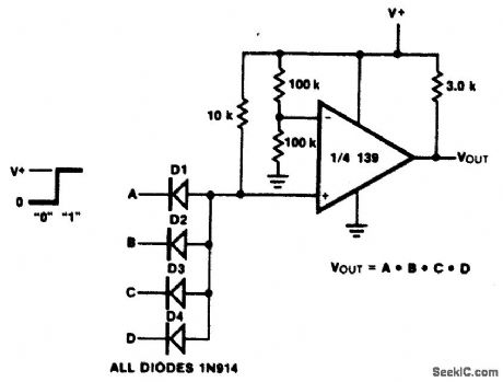
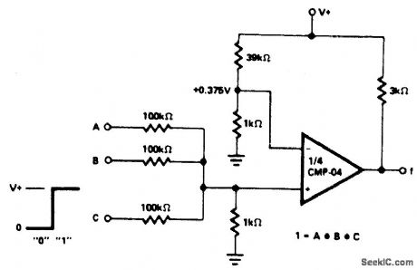
LARGE_FAN_IN_AND_GATE
Published:2009/6/25 3:18:00 Author:May
View full Circuit Diagram | Comments | Reading(785)
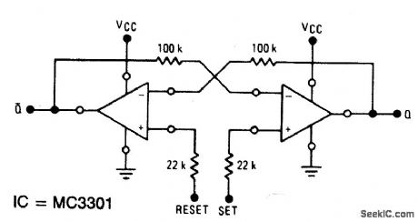
R_S_FLIP_FLOP
Published:2009/6/25 3:17:00 Author:May
View full Circuit Diagram | Comments | Reading(764)
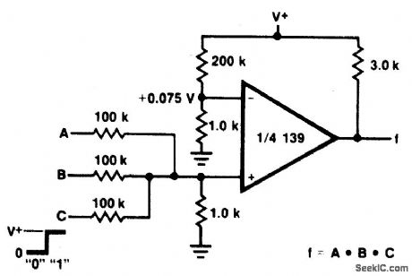
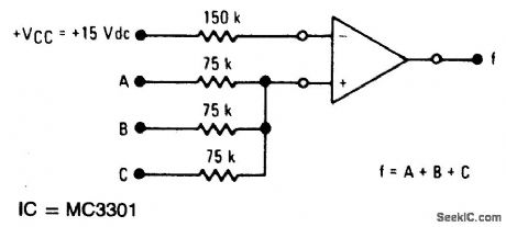
1OR_GATE
Published:2009/6/25 3:17:00 Author:May
View full Circuit Diagram | Comments | Reading(649)
AMMETER
Published:2009/6/25 3:16:00 Author:May
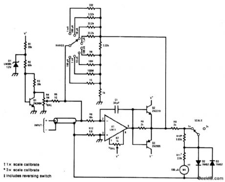
Circuit Notes
Current meter ranges from 100 pA to 3 mA full scale. Voltage across input is 100μV at lower ranges rising to 3 mV at 3 mA. The buffers on the op amp are to remove ambiguity with high-current overload, The output can also drive a DVM or a DPM. (View)
View full Circuit Diagram | Comments | Reading(3315)
AND_GATE
Published:2009/6/25 3:15:00 Author:May
View full Circuit Diagram | Comments | Reading(0)
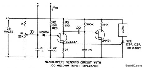
NANOAMPERE_SENSING_CIRCUIT_WITH_100_MEGOHM_INPUT_IMPEDANCE
Published:2009/6/25 3:29:00 Author:Jessie
Circuit Notes
The circuit may be used as a sensitive current detector or as a voltage detector having high input impedance. RI is set so that the voltage at point (A) is Vz to 3A volts below the level that fires the 2N494C. A small input cur-rent (Iin) of only 40 nanoamperes will charge C2 and raise the voltage at the emitter to the firing level. When the 2N494C fires, both capacitors, C1 and C2, are discharged through the 27 ohm resistor, which generates a positive pulse with sufficient amplitude to trigger a con-trolled rectifier (SCR), or other pulse sensitive circuitry. (View)
View full Circuit Diagram | Comments | Reading(1358)
OR_GATE___
Published:2009/6/25 3:14:00 Author:May
View full Circuit Diagram | Comments | Reading(652)
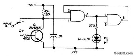
LOGIC_PROBE_1
Published:2009/6/25 4:15:00 Author:May
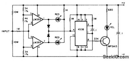
The probe indicates a high or low at 70% and 30% of V+ (5 to 12 V). One section of the voltage comparator (LM393) senses V in over 70% of supply and the second section senses V in under 30%. These two sections direct-drive the appropriate LEDs. The pulse detector is a CMOS oneshot (MC14538) triggered on the rising edge of the LM393 outputs through 1N4148 diodes. With the RC values shown, it triggered reliably at greater than 30 kHz on both sine and square waves. (View)
View full Circuit Diagram | Comments | Reading(4)
LOGIC_TEST_PROBE_WITH_MEMORY_
Published:2009/6/25 4:13:00 Author:May
There are two switches: a memory disable switch and a pulse polarity switch. Memory disable is a push-button that resets the memory to the low state when depressed. Pulse polarity is a toggle switch that selects whether the probe responds to a high-level or pulse (+5 V) or a low-level or pulse (ground). (Use IC logic of the same type as is being tested). (View)
View full Circuit Diagram | Comments | Reading(1034)
LOGIC_PROBE
Published:2009/6/25 4:12:00 Author:May
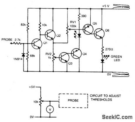
Transistors Q1 and Q2 form a buffer, pro-viding the probe with a reasonable input impe-dance. Q3 and Q4 form a level detecting circuit.As the voltage across the base-emitter junction of the Q3 rises above 0.6 V the transistor turns on thus turning on Q4 and lighting the red (high) LED. Q5 and Q6 perform the same function but for the green (low) LED. Q1, Q4, Q5 are all PNP general purpose silicon transistors (BC178 etc). Q2, Q3, Q6 are all PNP general purpose silicon transistors (BC 108 etc.) The threshold low is≤0.8 V, and the threshold high is≥2.4 V. (View)
View full Circuit Diagram | Comments | Reading(0)
NANO_AMMETER
Published:2009/6/25 3:25:00 Author:Jessie
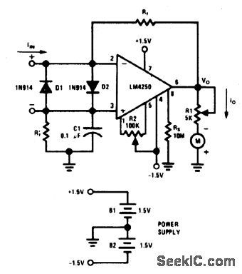
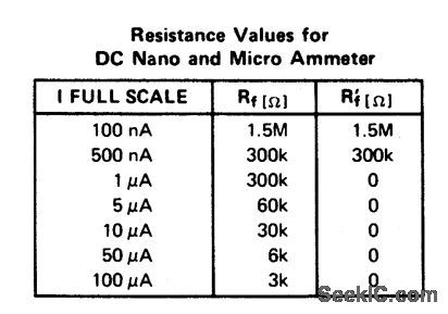
The complete meter amplifier is a differen-tial current-to-voltage converter with input pro-tection, zeroing and full scale adjust provisions, and input resistor balancing for minimum offset voltage. (View)
View full Circuit Diagram | Comments | Reading(2779)
AUDIBLE_TTL_PROBE
Published:2009/6/25 4:11:00 Author:May
When the probe is in contact with a TTL low (0) the probe emits a low note. With a TTL high (1), a high note is emitted. Power is supplied by the circuit under test. (View)
View full Circuit Diagram | Comments | Reading(776)
100_K_MEGOHM_DC_PROBE
Published:2009/6/25 4:10:00 Author:May
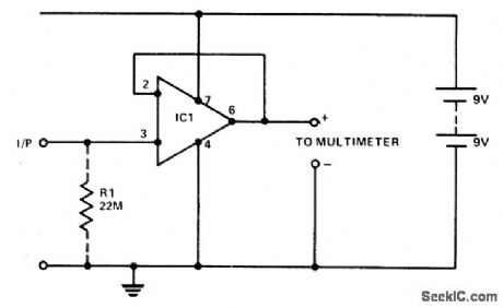
A 741 op amp is used with t00% ac and dc feedback to provide a typical input impedance of 1011 ohm and unity gain. To avoid hum and rf pickup the input leads should be kept as short as possible and the circuit should be mounted in a small grounded case. Output leads may belong since the output impedance of the circuit is a fraction of an ohm. With no input the output level is indeterminate. Including RI in the cir-cuit through lowers the input impedance to 22 M. (View)
View full Circuit Diagram | Comments | Reading(0)
RF_PROBE_FOR_VOM
Published:2009/6/25 4:09:00 Author:May
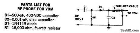
This probe makes possible relative measurements of rf voltages to 200 MHz on a 20,000 ohms-per-volt multimeter.Rf voltage must not exceed the breakdown rating of the IN4149-approximately 100 V. (View)
View full Circuit Diagram | Comments | Reading(0)
CMOS_LOGIC_PROBE
Published:2009/6/25 4:07:00 Author:May

The logic probe can indicate four input states, as follows: floating input-all LEDs off; logic 0 input-D2 switched on (D3 will briefly flash on); logic 1 input-Dl switched on; pulsing input-D3 switched on, or pulsing in the case of a low frequency input signal (one or both of the other indicators will switch on, showing if one input state predominates). (View)
View full Circuit Diagram | Comments | Reading(0)
INJECTOR_TRACER
Published:2009/6/25 4:06:00 Author:May
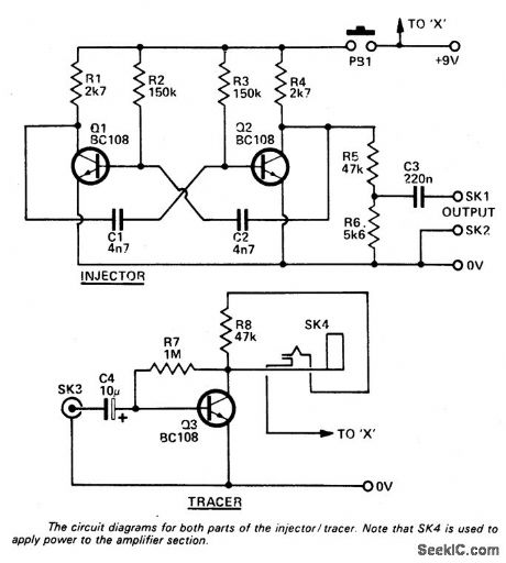
The unit has a separate amplifier and oscillator section allowing them to be used sepa-rately if need be. The injector is a multivibrator running at 1 kHz, with R5 and R6 dividing down the output to a suitable level (≈1V). The tracer is a single-stage amplifier that drives the high impedance earpiece. C4 decouples the input. (View)
View full Circuit Diagram | Comments | Reading(0)
PRECISION_1_μA_to_1_mA_CURRENT_SOURCES
Published:2009/6/25 4:06:00 Author:May
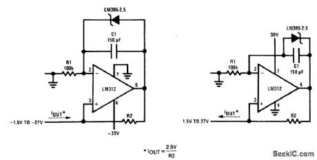
View full Circuit Diagram | Comments | Reading(694)
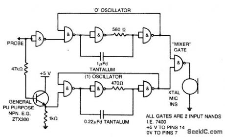
SIGNAL_INJECTOR_TRACER
Published:2009/6/25 4:04:00 Author:May
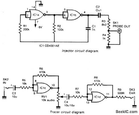
The injector is a CMOS oscillator with period approximately equal to 1.4 x C1 x R2 seconds. The values are given for 1 kHz opera-tion. Resistors R3 and R4 divide the output to 1 V. Whereas the oscillator employs the gates in their digital mode, the tracer used them in a linear fashion by applying negative feedback from output to input. They are used in much the same way as op amps. The circuit uses positiveground. It offers an advantage at the earphone output because one side of the earphone must be connected to ground via the case. Use of a positive ground allows the phone to be driven by the two N-channel transistors inside the CD4001 which are arranged in parallel and are thus able to handle more current for better volume. (View)
View full Circuit Diagram | Comments | Reading(0)
LOGIC_PROBE_YIELDS_THREE_DISCRETE_STATES
Published:2009/6/25 4:02:00 Author:May
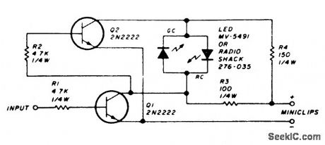
The circuit uses a dual LED. When power is applied to the probe through the power leads, and the input is touched to a low level or ground, Q1 is cut off. This will cause Q2 to conduct since the base is positive with respect to the emitter. With Q1 cut off and Q2 con-ducting, the greendiode ofthe dual LED will be forward biased, yielding a green output.Touching the probe tip to a high level will cause Q1 and Q2 to complement, and the red diode will be forward biased, yielding a red output from the LED. An alternating signal will cause alternating conduction of the red and green diodes and willyield an indication approxi-mately amber. In this manner, both static and dynamic signals can be traced with the logic probe. (View)
View full Circuit Diagram | Comments | Reading(0)
PRECISION_CURRENT_SOURCE
Published:2009/6/25 3:53:00 Author:May

Circuit Notes
The 2N5457 and PN2222 bipolar serve as voltage isolation devices between the output and the current sensing resistor, R1. The LM101 provides a large amount of loop gain to assure that the circuit acts as a current source. For small values of current (<1 mA), the PN2222 and 10K resistor may be eliminated with the outpuf appearing at the source of the 2N5457. (View)
View full Circuit Diagram | Comments | Reading(0)
| Pages:1308/2234 At 2013011302130313041305130613071308130913101311131213131314131513161317131813191320Under 20 |
Circuit Categories
power supply circuit
Amplifier Circuit
Basic Circuit
LED and Light Circuit
Sensor Circuit
Signal Processing
Electrical Equipment Circuit
Control Circuit
Remote Control Circuit
A/D-D/A Converter Circuit
Audio Circuit
Measuring and Test Circuit
Communication Circuit
Computer-Related Circuit
555 Circuit
Automotive Circuit
Repairing Circuit